Page History
| Scroll pdf ignore | |
|---|---|
|
Key Features
- Motor control evaluation with an suitable controller board
- Quick evaluation with reference motor board
- Power option up to 48V and 30A main supply current
...
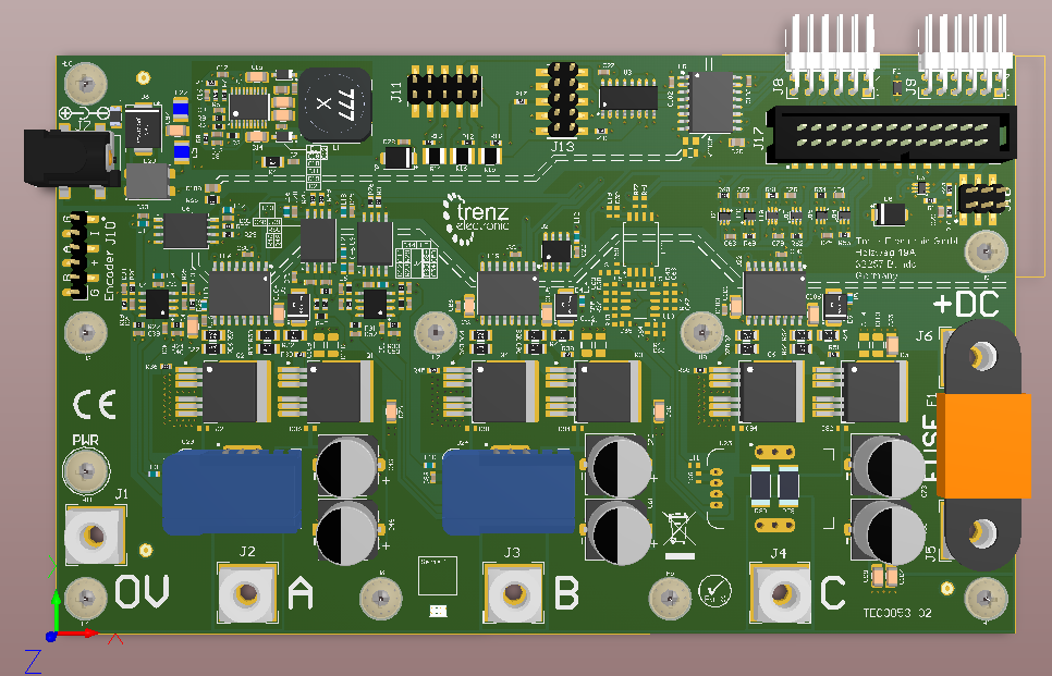
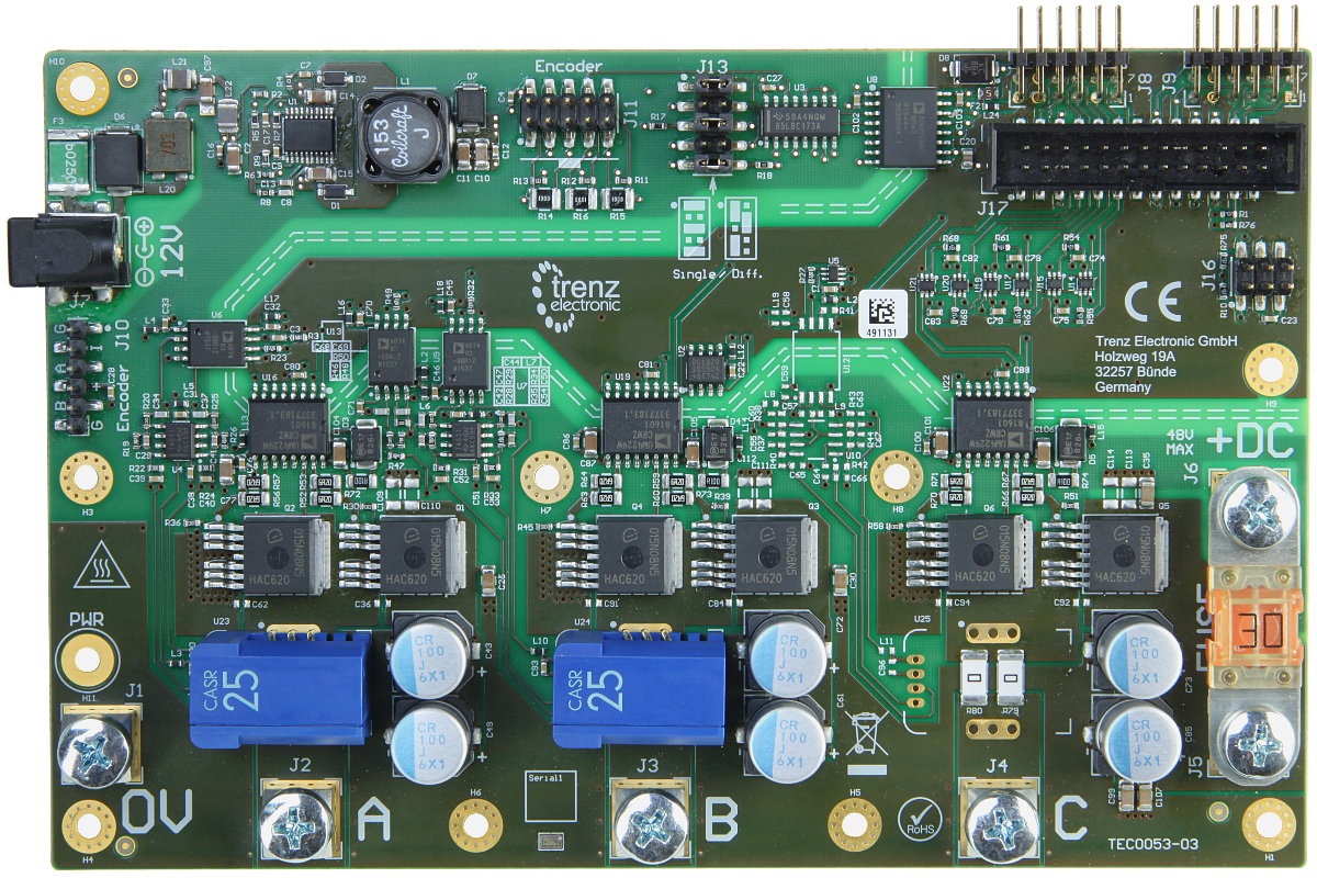
Control Board Connections
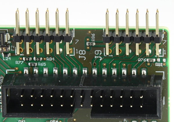
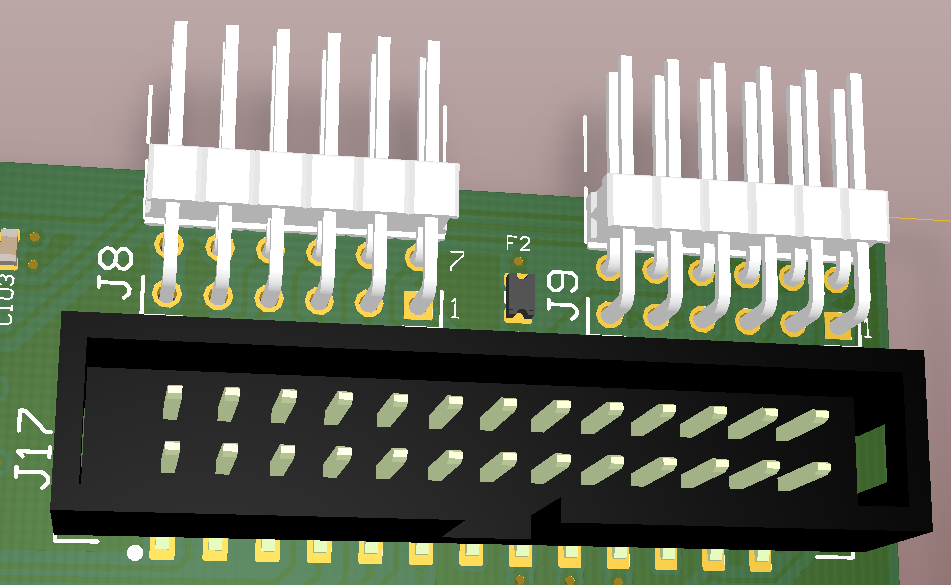
| Signal names | Connector J8 | Connector J9 | Connector J17 |
|---|---|---|---|
Digital Supply to EDPS | Pin 6, 12: +3.3V | Pin 6, 12: +3.3V Pin 5, 11: GND | Pin 5, 6, 21, 22: +3.3V Pin 1, 2, 25, 26: GND |
Motor Driver PWM Signals to EDPS High and Low Side control signals
| Pin 1: G1H - Ch.A HighSide | Pin 11: G1H - Ch.A HighSide | |
| ADC Clock Signal to EDPS | Pin 1: SCLK | Pin 23: SCLK | |
| Encoder Digital Signals from EDPS | Pin 8: ENC_A | Pin 20: ENC_A | |
| Motor Current ADC "raw" Signals from EDPS (usable with FPGA IP) | Pin 2: SDI1 - Current Ch.A | Pin 19: SDI1 - Current Ch.A | |
| Supply Voltage ADC "raw" Signal from EDPS (usable with FPGA IP) | Pin 7: SDIV - from DC_LINK | Pin 24: SDIV - from DC_LINK | |
| 1-Wire bus for temperature measurement | Pin 10: EXT1 - 1-Wire Bus 1 Pin 4: EXT2 - 1-Wire Bus 2 | Pin 4: EXT1 - 1-Wire Bus 1 | |
| Not connected pins | none | none | Pin 13, 14 |
...
Overview
Content Tools