Page History
...
This getting started guide covers system requirements, infrastructure, hardware test, reference designs and first reference switch project.
|
|

System Requirements
...
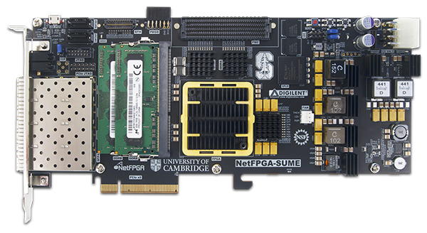
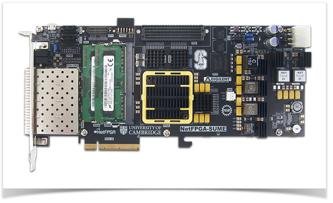
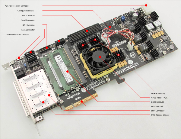
NetFPGA-SUME board
A micro-USB cable
4 unique MAC address stickers (one per 10G SFP+ Ethernet port)
The NetFGPA support package has:
...
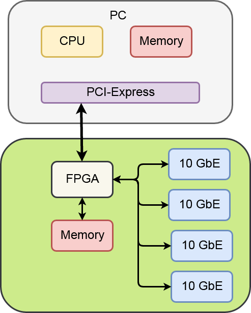
Some useful reference designs include reference NIC, reference router, reference switch and reference switch lite. For example, NetSUME-FPGA will act as a learning switch if the reference switch project is loaded on the board. The incoming packets will be transmitted to the corresponding output ports, based on MAC address. Figure 1 shows the internal structure.
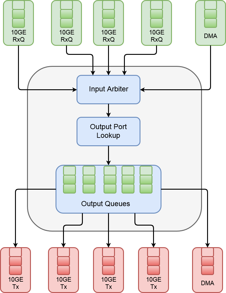
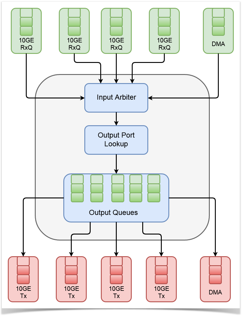
Figure 1
The switching process can be broken down into five stages:
...
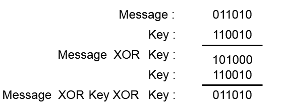
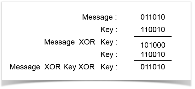
After the user understand the basic concept and underlying principle, they can modify the switch to encrypt the received data using one time pad method: make a XOR between the Message and a key K.
User can implement a Verilog module that makes the encryption and decryption of the payload. It was designed as a finite state machine (three states) to detect the header, which remains as it is, and the payload. This module was packaged as an IP and will be introduced in the switch pipeline. There are two ways to integrate the obtained IP into the main project. The block diagram (block design) is for someone who is familiar with Vivado block design. The Tcl script is good for version control or letting user understand Vivado GUI.
...
After the encryption, Figure 2 shows the modified structure called Crypo-Switch.
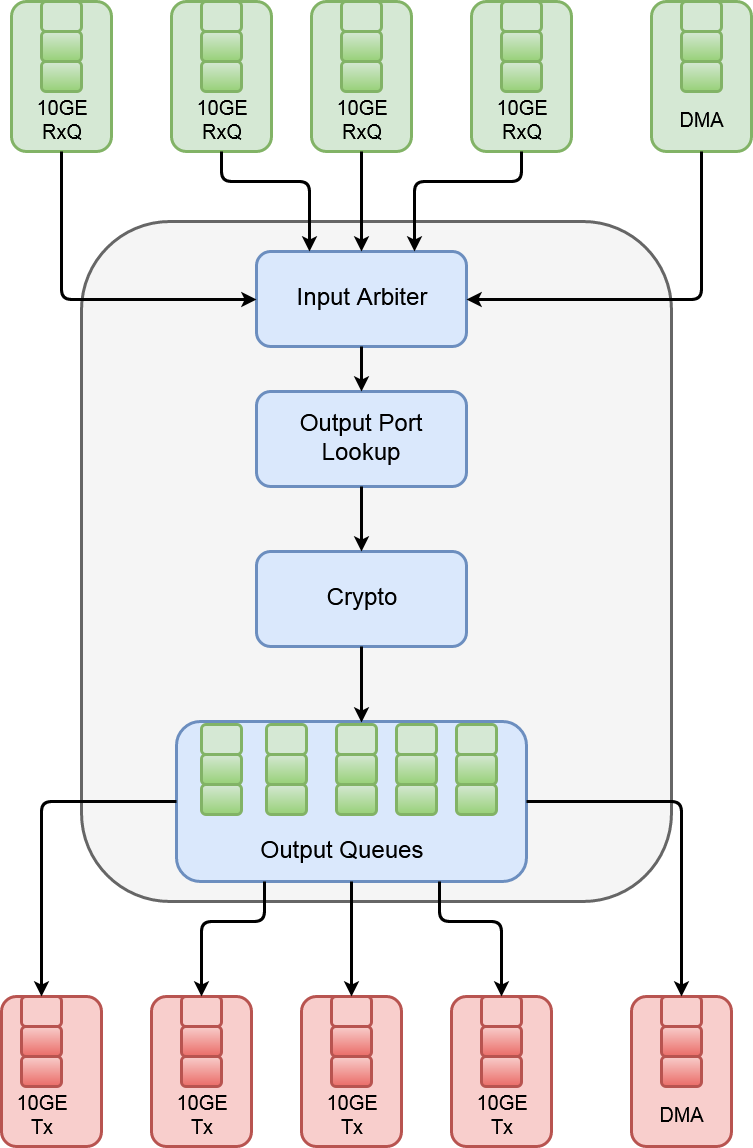
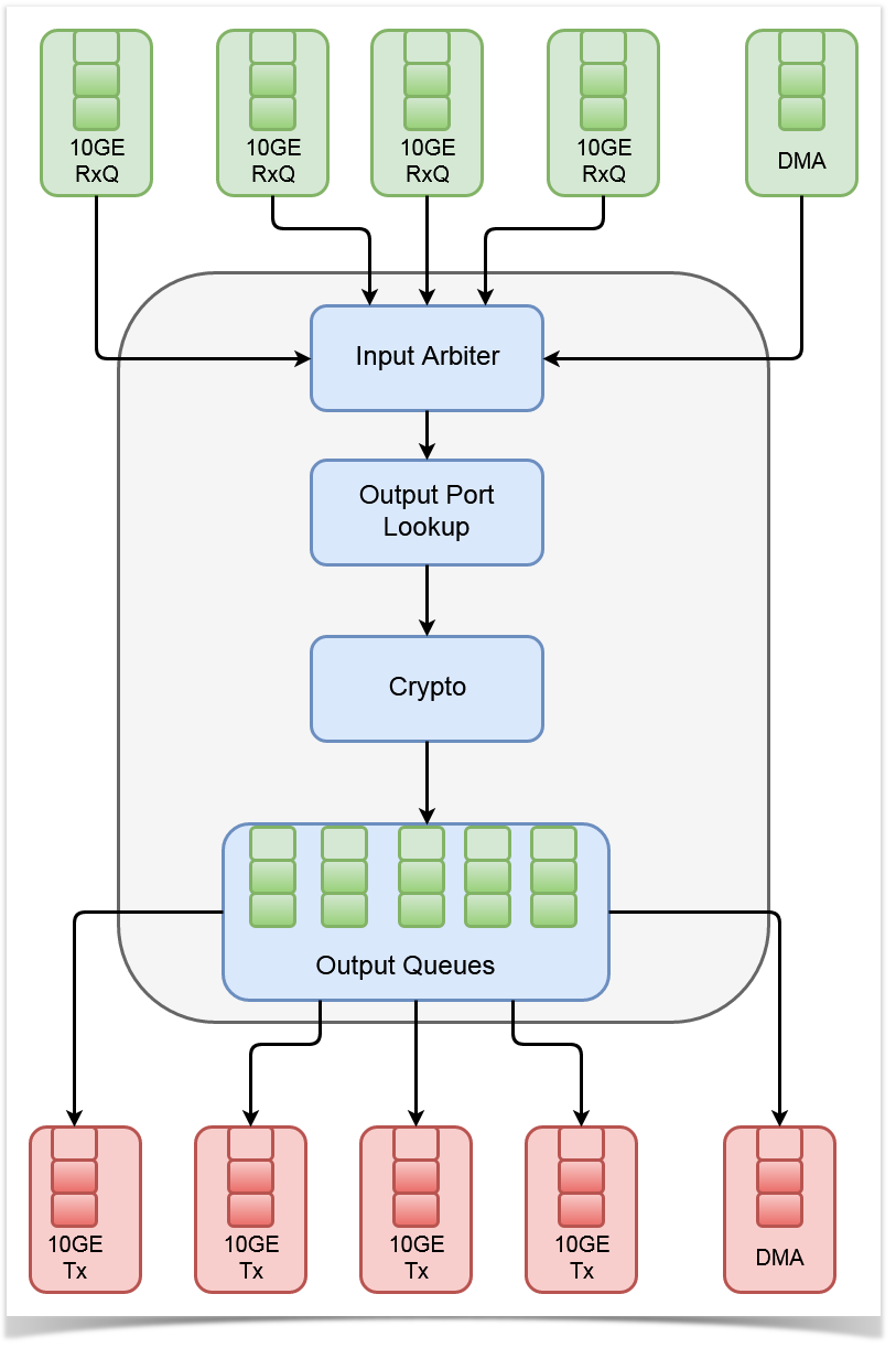
Figure 2
Now, user can run the simulation and debug the design. The simulation allows user to test the design without requiring lengthy synthesis process. Because the NetSUME-FPGA board has a complex FPGA architecture, the bitstream generation process takes more than 45 minutes. The simulation will be run in Vivado Simulator. To generate Ethernet packets, we used Scapy. The details is at https://github.com/NetFPGA/NetFPGA-SUME-public/wiki/NetFPGA-SUME-Simulations .
Once the user validate the design through simulation, they can generate the bitstream and upload it on the board. This approach is suitable for digital designers who know Verilog or VHDL and aim a high-performance system. For a software engineer or someone who want to parse the incoming data and take action based on the packet header or payload, they should use P4. P4 is a high level programming language that is used to describe packet processing logic and to implement forwarding-plane of network elements. Users can describe the logic in P4 and use Xilinx SDNet. The code can be compiled under Xilinx SDNet and the complied design can be uploaded in NetSUME-FPGA. There is a simple switch example based for NetFGPA SUME in Xilinx SDNet (/opt/Xilinx/SDNet/<version_number>/data/p4include/sume_switch.p4). Figure 3 shows the switch architecture.
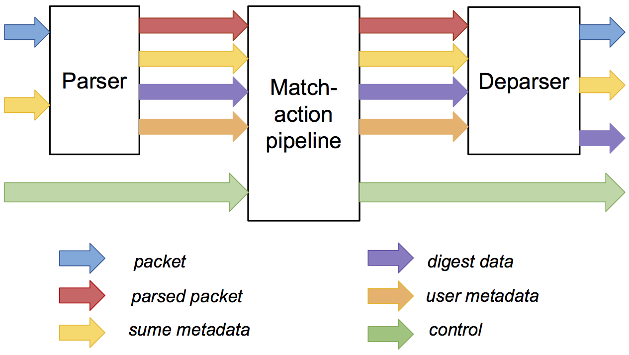
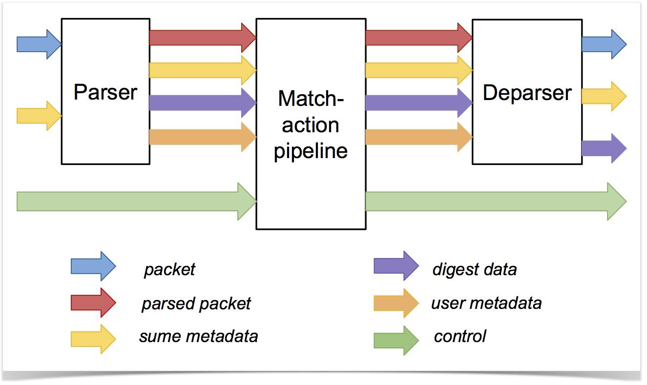
Figure 3
References
NetFPGA Summer School courses: https://www.cl.cam.ac.uk/research/srg/netos/projects/netfpga/workshop/summer-school-2017/
NetFPGA Wiki: https://github.com/NetFPGA/NetFPGA-SUME-public/wiki
Ordering NetFPGA SUME
Overview
Content Tools