Page History
...
Figure 1: TEBA0841-01 Block Diagram.
Main Components
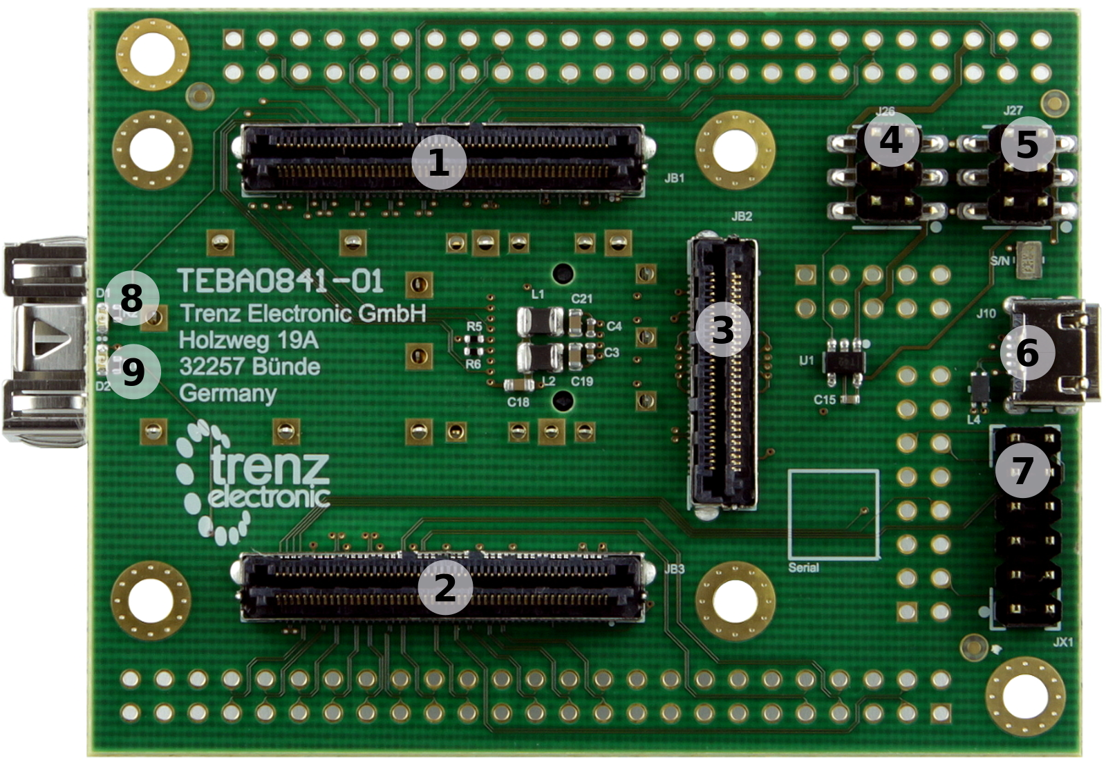
Figure 2: TEBA0841-01 Carrier Board.
...
Table 5: JTAG interface signals.
UART Interface
UART interface is available on B2B connector JB1 and is usually established by MIO-pins of the PS-bank of the mounted SoM's Zynq device. With the TE0790 XMOD USB2.0 adapter, the UART signals can be converted to USB2.0 interface signals:
XMOD FTDI JTAG-Adapter Header
The JTAG interface of the mounted SoM can be accessed via XMOD header JX1, so in use with the XMOD-FT2232H adapter-board TE0790 the mounted SoM can be programmed via USB2.0 interface. The TE0790 board provides also an UART interface to the SoM's Zynq device which can be accessed by the USB2.0 interface of the adapter-board while the signals between these serial interfaces will be converted.
Following table describes the signals and interfaces of the XMOD header JX1:
| Pin Schematic Name | XMOD Header JX1 Pin | B2B | Note |
|---|---|---|---|
| TCK | C (pin 4) | JB3-100 | - |
| TDO | D (pin 8) | JB3-98 | - |
| TDI | F (pin 10) | JB3-96 | - |
| TMS | H (pin 12) | JB3-94 | - |
| MIO15 | A (pin 3) | JB1-86 |
| UART-TX (transmit line) | |
| MIO14 | B (pin 7) |
Table 6: UART interface signals.
SD IO Interface
The SD IO interface of the mounted SoM is routed to the pin header J4. Due to the different operation voltage levels of the MicroSD Card socket (3.3V) and the and the SoM's Zynq device MIO-bank (1.8V), a VDD/VCCIO translation is necessary which can be provided for example by Texas Instruments TXS02612 SDIO port expander IC. Both voltage levels are available on pin header J4:
...
Table 7: SD IO interface signals.
USB2.0 Interface
TEBA0841 board has one physical Micro USB2.0 type B socket J10, the differential data signals of the USB2.0 socket are routed to the B2B connector JB2, where they can be accessed by the corresponding USB2.0 PHY transceiver of the mounted SoM.
With Micro USB2.0 type B socket, the USB2.0 interface can also be used in Device or OTG mode.
Following table gives an overview of the USB2.0 interface signals:
...
JB2-48
...
Table 8: USB2.0 interface signals and connections.
XMOD FTDI JTAG-Adapter Header
The JTAG interface of the mounted SoM can be accessed via XMOD header JX1 and pin header J3, which has a 'XMOD FTDI JTAG Adapter'-compatible pin-assignment, but also two additional pins (15,16) as differential pairs to supply the mounted SoM with an external MGT reference clock signal.
So in use with the XMOD-FT2232H adapter-board TE0790 the mounted SoM can be programmed via USB2.0 interface. The TE0790 board provides also an UART interface to the SoM's Zynq device which can be accessed by the USB2.0 interface of the adapter-board while the signals between these serial interfaces will be converted.
Following table describes the signals and interfaces of the XMOD header JX1 and pin header J3:
...
When using XMOD FTDI JTAG Adapter TE0790, the adapter-board's VCC and VCCIO will be sourced by the on-boards 3.3V supply voltage. Set the DIP-switch with the setting:
...
Use Xilinx compatible TE0790 adapter board (designation TE-0790-xx with out 'L') to program the Xilinx Zynq devices.
...
| JB1-91 | UART-RX (receive line) | ||
| BOOTMODE | E (pin 9) | JB1-90 | JTAGSEL at TE 4 x 5 SoMs standard pin assignment |
| RESIN | G (pin 11) | JB3-17 | System Reset at TE 4 x 5 SoMs standard pin assignment |
Table 6: XMOD header JX1 signals and connections.
When using XMOD FTDI JTAG Adapter TE0790, the adapter-board's VCC and VCCIO will be sourced by the on-boards 3.3V supply voltage. Set the XMOD DIP-switch with the setting:
| XMOD DIP-switches | Position |
|---|---|
| Switch 1 | ON |
| Switch 2 | OFF |
| Switch 3 | OFF |
| Switch 4 | OFF |
Table 7: XMOD adapter board DIP-switch positions for voltage configuration.
| Note |
|---|
Use Xilinx compatible TE0790 adapter board (designation TE-0790-xx with out 'L') to program the Xilinx Zynq devices. The TE0790 adapter board's CPLD have to be configured with the Standard variant of the firmware. Refer to the TE0790 Resources Site for further information and firmware download. |
JTAG/UART header J3
As alternative to the XMOD header JX1, on the Carrier Board pin header J3 is present, which has a XMOD header-compatible pin-assignment, but also two additional pins (15,16) as differential pairs to supply the mounted SoM with an external MGT reference clock signal:
| Pin Schematic Name | Header J3 Pin | B2B | Note |
|---|---|---|---|
| TCK | 4 | JB3-100 | - |
| TDO | 8 | JB3-98 | - |
| TDI | 10 | JB3-96 | - |
| TMS | 12 | JB3-94 | - |
| MIO15 | 3 | JB1-86 | UART-TX (transmit line) |
| MIO14 | 7 | JB1-91 | UART-RX (receive line) |
| BOOTMODE | 9 | JB1-90 | usually 'JTAGSEL' on TE 4 x 5 SoMs |
| RESIN | 11 | JB3-17 | SoM Reset pin |
| CLK0_N | 15 | JB2-32 | AC decoupled on-board (100 nF capacitor) |
| CLK0_P | 16 | JB2-34 | AC decoupled on-board (100 nF capacitor) |
Table 8: JTAG/UART header J3 signals and connections.
UART Interface
UART interface is available on B2B connector JB1 and is usually established by MIO-pins of the PS-bank of the mounted SoM's Zynq device. With the TE0790 XMOD USB2.0 adapter, the UART signals can be converted to USB2.0 interface signals:
| UART Signal Schematic Name | B2B | XMOD Header JX1 | Pin Header J3 | Note |
|---|---|---|---|---|
| MIO14 | JB1-91 | JX1-7 | J3-7 | UART-RX (receive line) |
| MIO15 | JB1-86 | JX1-3 | J3-3 | UART-TX (transmit line) |
Table 9: UART interface signals.
SD IO Interface
The SD IO interface of the mounted SoM is routed to the pin header J4. Due to the different operation voltage levels of the MicroSD Card socket (3.3V) and the and the SoM's Zynq device MIO-bank (1.8V), a VDD/VCCIO translation is necessary which can be provided for example by Texas Instruments TXS02612 SDIO port expander IC. Both voltage levels are available on pin header J4:
| SD IO Signal Schematic Name | B2B | Pin Header J4 | Note |
|---|---|---|---|
| SD_DAT0 | JB1-24 | J4-8 | SD IO data |
| SD_DAT1 | JB1-22 | J4-10 | SD IO data |
| SD_DAT2 | JB1-20 | J4-9 | SD IO data |
| SD_DAT3 | JB1-18 | J4-7 | SD IO data |
| SD_CLK | JB1-28 | J4-4 | SD IO clock |
| SD_CMD | JB1-26 | J4-3 | SD IO command |
Table 7: SD IO interface signals.
USB2.0 Interface
TEBA0841 board has one physical Micro USB2.0 type B socket J10, the differential data signals of the USB2.0 socket are routed to the B2B connector JB2, where they can be accessed by the corresponding USB2.0 PHY transceiver of the mounted SoM.
With Micro USB2.0 type B socket, the USB2.0 interface can also be used in Device or OTG mode.
Following table gives an overview of the USB2.0 interface signals:
| USB2.0 Signal Schematic Name | B2B | Connected to | Note |
|---|---|---|---|
| OTG_N | JB2-48 | J10-2 | USB2.0 data |
| OTG_P | JB2-50 | J10-3 | USB2.0 data |
| OTG-ID | JB2-52 | J10-4 | Ground this pin for A-Device (host), left floating this pin for B-Device (peripheral). |
| USB-VBUS | JB2-56 | J10-1 | USB supply voltage for Host mode. Not supplied by the Carrier Board. |
Table 8: USB2.0 interface signals and connections.
On-board Peripherals
| HTML |
|---|
<!-- Components on the Module, like Flash, PLL, PHY... --> |
...
| On-board Pin Header Designator | VCC / VCCIO | Direction | Pins | Notes |
|---|---|---|---|---|
| J17 | 3.3V | In / Out | 5, 48 | 3.3V external supply voltage |
| VCCIOD | In / Out | 6, 45 | PL IO-bank VCCIO, depends on Jumper settings | |
| J20 | 3.3V | In / Out | 5, 48 | 3.3V external supply voltage |
| VCCIOA | In / Out | 6, 45 | PL IO-bank VCCIO, depends on Jumper settings | |
| J4 | 3.3V | Out | 5 | - |
| M1.8VOUT | Out | 6 | - |
Table 17: Power Pin description of on-board connector.
...
| Jumper / Header Designator | VCC / VCCIO | Direction | Pins | Notes | ||||
|---|---|---|---|---|---|---|---|---|
| J26 | VCCIOA | In | 2, 4, 6 | - | ||||
| M1.8VOUT | Out | 1 | - | |||||
| 2.5V | Out | 3 | - | |||||
| 3.3V_OUT | Out | 5 | - | |||||
| J27 | VCCIOD | In | 2, 4, 6 | - | ||||
| M1.8VOUT | Out | 1 | - | |||||
| 2.5V | Out | 3 | - | |||||
| 3.3V_OUT | Out | 5 | - | J4 | 3.3V | Out | 5 | - |
| M1.8VOUT | Out | 6 | - |
Table 18: Power Pin description of VCCIO selection jumper pin header.
...
Table 19: Power pin description of peripheral connector.
| XMOD JTAG Header Designator | VCC / VCCIO | Direction | Pins | Notes |
|---|---|---|---|---|
| JX1 (XMOD) | 3.3V | Out | 5 | connected connected to 3.3V external supply voltage |
| VIO | Out | 6 | ||
| J3 | 3.3V | Out | 5 | connected to 3.3V external supply voltage |
| 3.3V | Out | 6 |
...
Overview
Content Tools