Page History
...
Figure 1: TEBA0841-01 Block Diagram.
Main Components
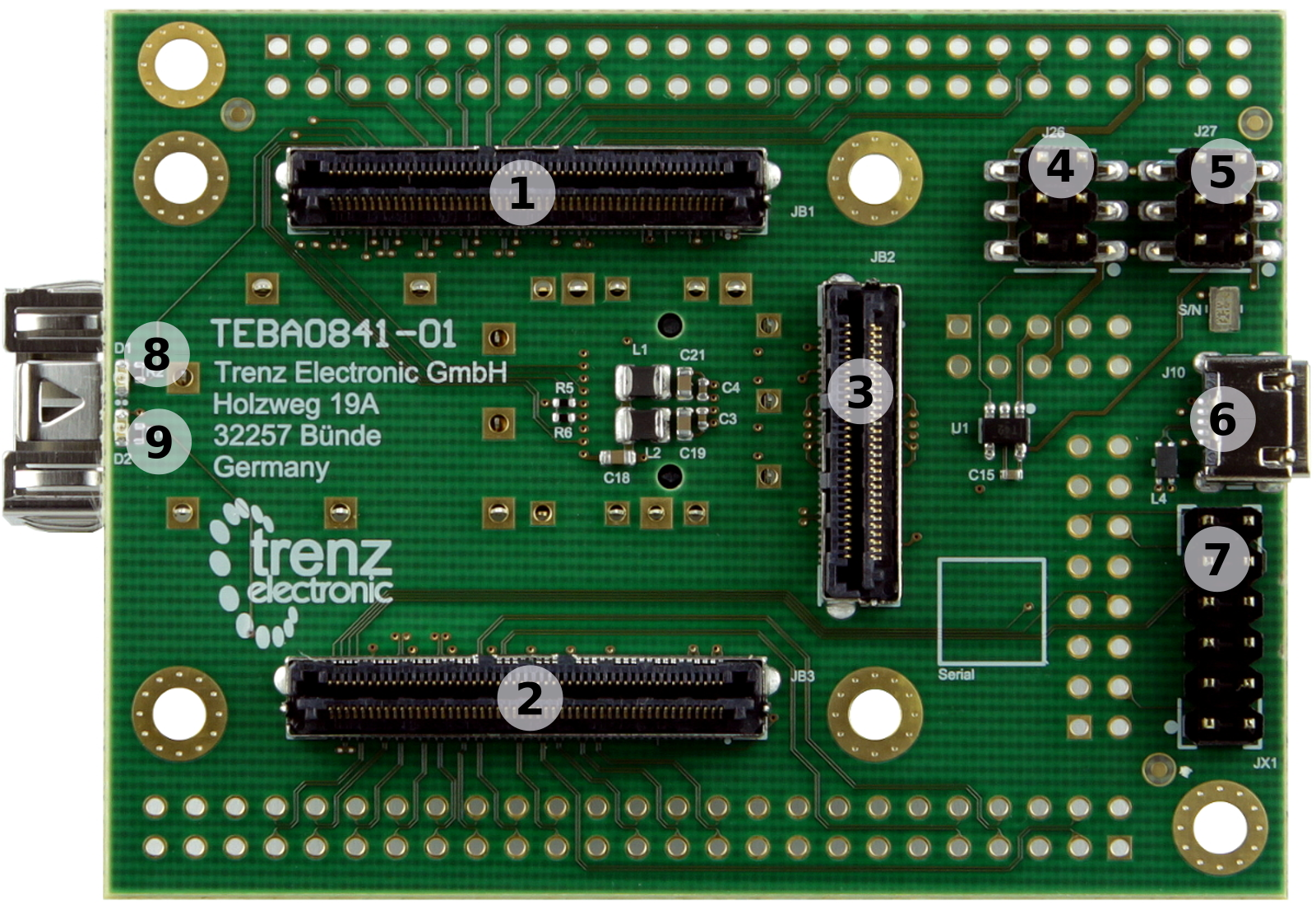
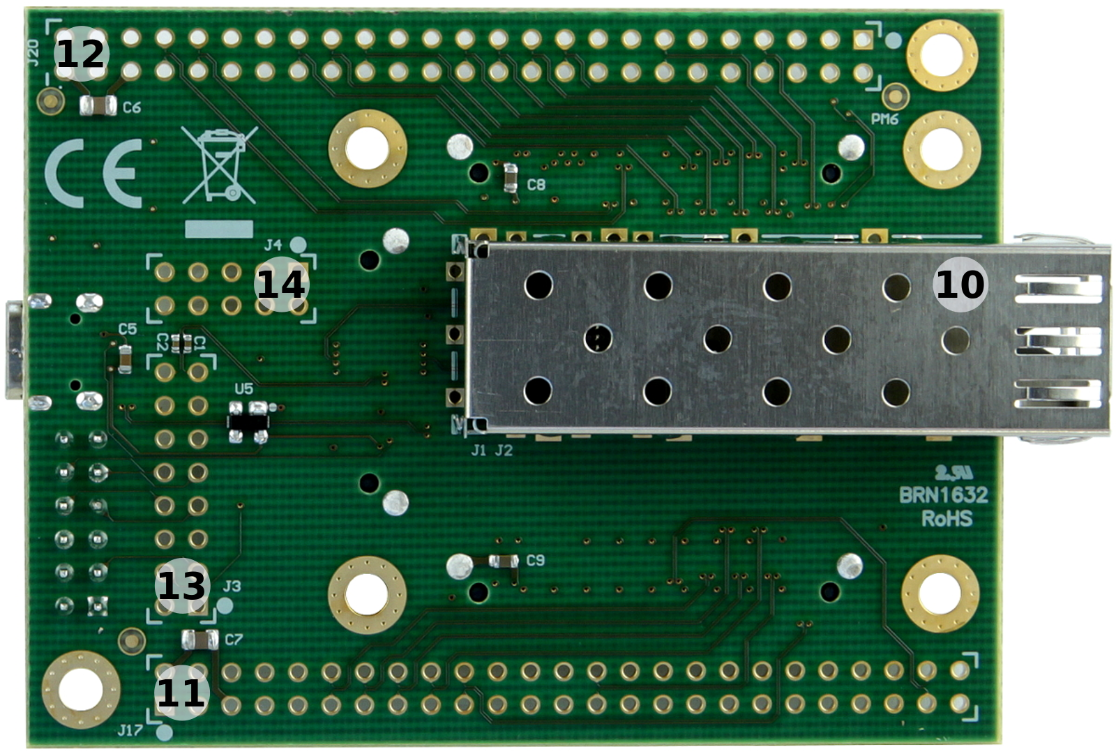
Figure 2: TEBA0841-01 Carrier Board.
...
Following table describes the signals and interfaces of the XMOD header JX1:
| Pin Schematic Name | XMOD Header JX1 Pin | B2B | Note |
|---|---|---|---|
| TCK | C (pin 4) | JB3-100 | - |
| TDO | D (pin 8) | JB3-98 | - |
| TDI | F (pin 10) | JB3-96 | - |
| TMS | H (pin 12) | JB3-94 | - |
| MIO15 | A (pin 3) | JB1-86 | UART-TX (transmit line) |
| MIO14 | B (pin 7) | JB1-91 | UART-RX (receive line) |
| BOOTMODE | E (pin 9) | JB1-90 | JTAGSEL at TE 4 x 5 SoMs standard pin assignment |
| RESIN | G (pin 11) | JB3-17 | System Reset at TE 4 x 5 SoMs standard pin assignment |
Table 6: XMOD header JX1 signals and connections.
When using XMOD FTDI JTAG Adapter TE0790, the adapter-board's VCC and VCCIO will be sourced by the on-boards 3.3V supply voltage. Set the XMOD DIP-switch with the setting:
| XMOD DIP-switches | Position |
|---|---|
| Switch 1 | ON |
| Switch 2 | OFF |
| Switch 3 | OFF |
| Switch 4 | OFF |
Table 7: XMOD adapter board DIP-switch positions for voltage configuration.
...
As alternative to the XMOD header JX1, on the Carrier Board pin header J3 is present, which has a XMOD header-compatible pin-assignment, but also two additional pins (15,16) as differential pairs to supply the mounted SoM with an external MGT reference clock signal:
| Pin Schematic Name | Header J3 Pin | B2B | Note |
|---|---|---|---|
| TCK | 4 | JB3-100 | - |
| TDO | 8 | JB3-98 | - |
| TDI | 10 | JB3-96 | - |
| TMS | 12 | JB3-94 | - |
| MIO15 | 3 | JB1-86 | UART-TX (transmit line) |
| MIO14 | 7 | JB1-91 | UART-RX (receive line) |
| BOOTMODE | 9 | JB1-90 | usually 'JTAGSEL' on TE 4 x 5 SoMs |
| RESIN | 11 | JB3-17 | SoM Reset pin |
| CLK0_N | 15 | JB2-32 | AC decoupled on-board (100 nF capacitor) |
| CLK0_P | 16 | JB2-34 | AC decoupled on-board (100 nF capacitor) |
Table 8: JTAG/UART header J3 signals and connections.
...
Overview
Content Tools