Page History
...
| Scroll pdf ignore | |
|---|---|
Table of Contents
|
Overview
| Scroll Only (inline) |
|---|
Refer to https://wiki.trenz-electronic.de/display/PD/TE0725LP+TRM for online version of this manual and the rest of available documentation of the product. |
The Trenz Electronic TE0725LP is a low cost small-sized FPGA module integrating a Xilinx Artix-7 and 32 MByte Flash memory for configuration and operation.
...
Xilinx Artix-7 XC7A100T FPGA
32 MByte Flash memory
2 x 50-pin headers with 2,54mm pitch, ideal for breadboard use
- 92 x GPIOs (42 + 42 + 8)
- 25.000000 MHz system clock
- I2C EEPROM for FPGA bitstream
3.3V single power supply with on-board voltage regulators
JTAG/UART connector
1 user LED
- Optional HyperRAM (8 to 32 MByte)
- Commercial temperature grade (Industrial on Request)
- Size 73 x 35 mm
Block Diagram
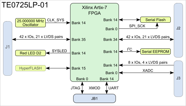
Figure 1: TE0725LP-01 Block Diagram.
| Page break |
|---|
Main Components
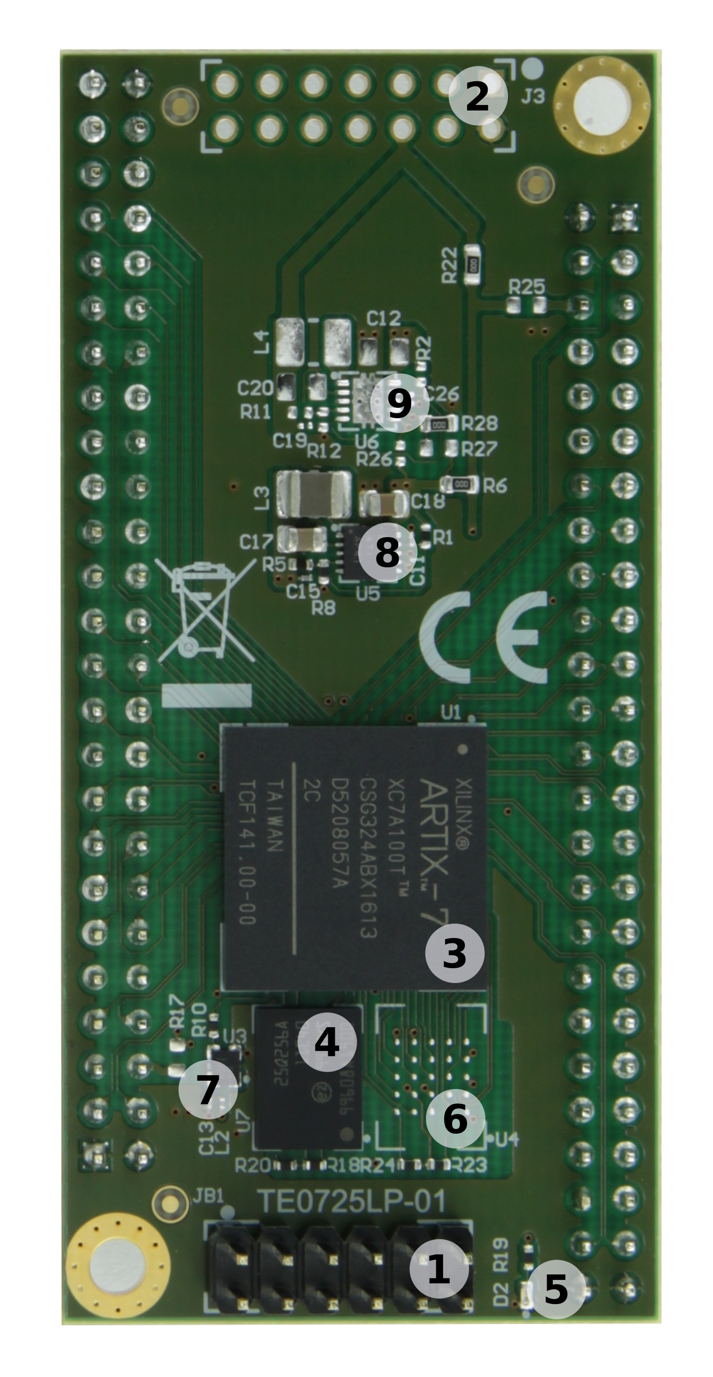
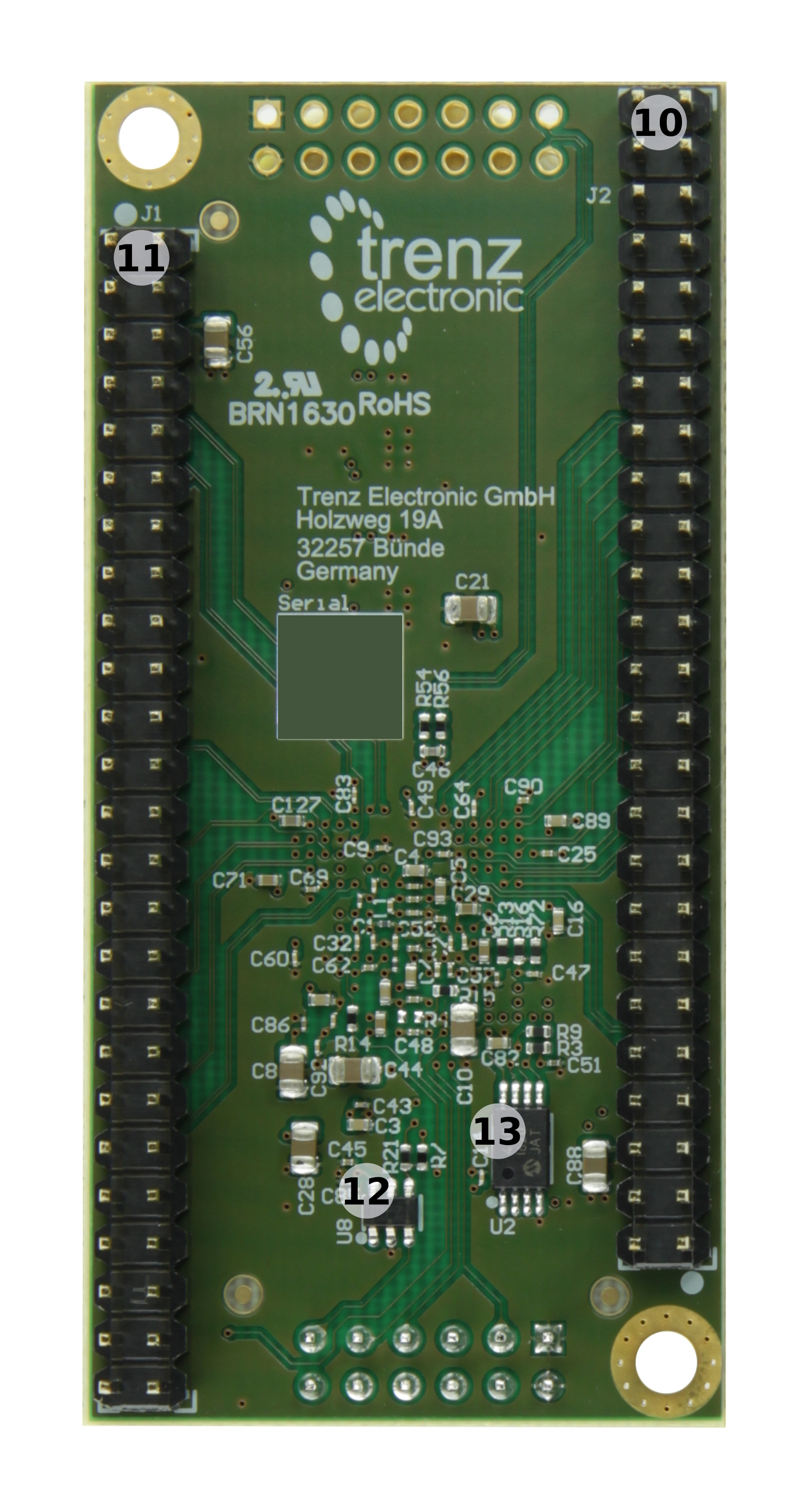
Figure 2: TE0725LP-01 FPGA module.
- XMOD header, JB1
- 14-pin header placeholder for connector, J3
- Xilinx Artix-7 FPGA, U1
- 128K I2C CMOS serial EEPROM, U2
- 1.8V, 256 MBit (32 MByte) quad SPI serial flash memory, U7
- Red LED (SYSLED), D2Low-power programmable oscillator @25.000000 MHz, U3
- Cypress S26KS512S 512 - Mbit (64 - MByte) 1.8V HyperFlash™ memory, U4
- Low-power programmable oscillator @25.000000 MHz, U3
- Low VIN high-efficiency step-down converter (1.5A max.), U5
- Low VIN high-efficiency step-down converter (1.5A max.), U6
- 1.8V, 256-MBit (32-MByte) quad SPI serial flash memory, U7
- Ultra-low supply-current voltage monitor with optional watchdog, U8
- 50-pin header placeholder for breadboard connector, J1
- 50-pin header placeholder for breadboard connector, J2
- 14-pin header placeholder for connector, J3
- JTAG/UART connector, JB1
- Ultra-low supply-current voltage monitor with optional watchdog, U8
- 128K I2C CMOS serial EEPROM, U2Red LED (SYSLED), D2
Initial Delivery State
| On-board Programmable Device | Content | Notes |
|---|---|---|
| Quad SPI Flash (U7) OTP area | Empty | - |
| I2C EEPROM, U2 | Empty | - |
| HyperFlash™ memory, U4 | Empty | - |
Table 1: Module initial delivery state of programmable on-board devices.
Boot Process
Boot...By default the configuration mode pins of the FPGA are set to QSPI mode, hence the FPGA is configured from serial NOR flash at system start-up. The JTAG interface of the module is provided for storing the initial FPGA configuration data to the QSPI flash memory.
Signals, Interfaces and Pins
...
JTAG access to the Xilinx Artix-7 device is provided through connector JB1.
| Signal | Pin Number |
|---|---|
| TCK | JB1-4 |
| TDO | JB1-8 |
| TDI | JB1-10 |
| TMS | JB1-12 |
...
Variants Currently In Production
| Module Variant | FPGA Chip Model | PL Clock | VIN Supply Voltage |
|---|---|---|---|
| TE0725LP-01-100-2C | XC7A100T-2CSG324C | 25 MHz | 3.3 V |
| TE0725LP-01-100-2D | XC7A100T-2CSG324C | 25 MHz | 1.8 V |
| TE0725LP-01-100-2L | XC7A100T-2CSG324C | 25 MHz | 1.8 V |
Technical Specifications
Absolute Maximum Ratings
Parameter | Min | Max | Units | Reference document |
|---|---|---|---|---|
3.3V supply voltage | -0.1 | 3.6 | V | |
| HR I/O banks supply voltage (VCCO) | -0.5 | 3.6 | V | Xilinx datasheet DS181 |
| HR I/O banks input voltage | -0.4 | VCCO + 0.55 | V | Xilinx datasheet DS181 |
Storage Temperature | -40 | +85 | °C |
Recommended Operating Conditions
| Parameter | Min | Max | Units | Reference document |
|---|---|---|---|---|
| VIN supply voltage | 3.135 | 3.45 | V | |
| HR I/O banks supply voltage (VCCO) | 1.14 | 3.465 | V | Xilinx datasheet DS181 |
| HR I/O banks input voltage | -0.20 | VCCO + 0.20 | V | Xilinx datasheet DS181 |
| Operating Temperature | 0 | +85 | °C |
| Note |
|---|
| Please check Xilinx datasheet DS181 for complete list of absolute maximum and recommended operating ratings for the Artix-7 device. |
...
Hardware Revision History
| Date | Revision | Notes | PCN | Documentation Link |
|---|---|---|---|---|
| 2016-07-21 | 01 | Prototypes |
Hardware revision number is printed on the PCB board together with the module model number separated by the dash.
...
Overview
Content Tools