Page History
...
Intel Cyclone 10LP 10CL025 FPGA SoC
- 8 MByte SDRAM
2 MByte serial configuration memory
- ST Microelectronics LIS3DH 3-axis accelerometer
- JTAG and UART over Micro USB2 connector
- 1x6 pin header for JTAG access to FPGA SoC
- 1x PMOD header providing 8 GPIOs
2x 14-pin headers (2,54 mm pitch) providing 23 GPIOs
- 1x 3-pin header providing 2 GPIOs
8x user LEDs
- 1x user push button
- 35.3V 0V single power supply with on-board voltage regulators
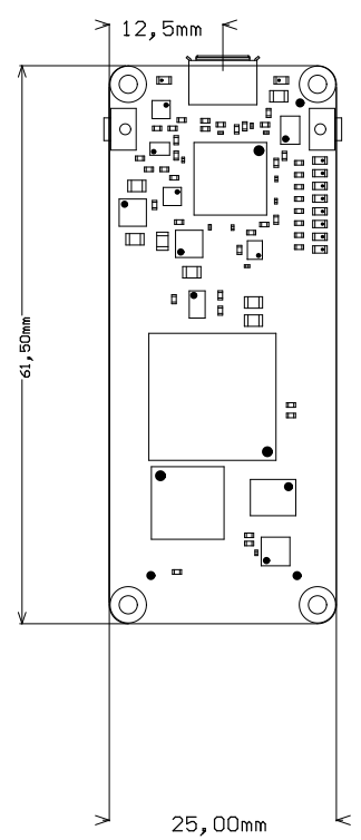
- Size: 61.5 x 25 mm
...
- Intel Cyclone 10LP 10CL025 FPGA SoC, U1
- Winbond W9864G6JT 8 Mbyte SDRAM 166MHz, U2
- Intel EPCQ16ASI8N 2 MByte serial configuration memory, U5
- ST Microelectronics LIS3DH 3-axis accelerometer, U4
- FTDI USB2 to JTAG/UART adapter, U3
- Configuration EEPROM for FTDI chip, U9
- 12.0000 MHz oscillator, U7
- 8x red user LEDs, D2 ... D9
- Red LED (Conf. DONE), D10
- Green LED (indicating supply voltage), D1
- Push button (user), S2
- Push button (reset), S1
- Micro USB2 B socket (receptacle), J9
- 1x14 pin header (2.54mm pitch), J2
- 1x6 pin header (2.54mm pitch), J4
- 2x6 Pmod connector, J6
- 3-pin header (2.54mm pitch), J3
- 1x14 pin header (2.54mm pitch), J1
...
By default the configuration mode pins of the FPGA are set to load the FPGA design from the serial configuration memory, hence the FPGA is configured from serial configuration memory at system start-up. The JTAG interface of the module is provided for storing the initial FPGA configuration data to the serial configuration memory.
...
Table 2: General overview of single ended I/O signals connected to pin headers and connectors
FPGA I/O banks
| BankVCCIO | I/O's Count | Connected to | Notes | ||
|---|---|---|---|---|---|
| 13.3V | 6 | LIS3DH digital motion sensor, U4 | SPI interface, 2 interrupt lines | ||
| 4 | 1x6 pin header, J4 | JTAG interface | |||
| 4 | 2 MByte serial configuration memory, U5 | FPGA configuration memory with active serial (AS) x1 interface | |||
| 1 | J2-10, push button S1 | low active reset input | |||
| 23.3V | 9 | 1x14 pin header, J2 | GPIOs (2 I/O's of bank 2 can be pulled-up to 3.3V (4K7 resistors) with 2 I/O's of same Bank or pins can be shared) | 3||
| 3.3V | 8 | LEDs D2 ... D9 | 8 x red user LEDs | ||
| 8 | FTDI FT2232H JTAG/UART Adapter, U3 | configurable as GPIO/UART or other serial interfaces | |||
| 1 | push button S2 | user button | |||
| 4 | 3.3V | 10 | pin headers J1, J3 | GPIOs | |
| 53.3V | 6 | pin headers J1 | GPIOs | ||
| 63.3V | 8 | Pmod connector J6 | GPIOs | ||
| 1 | Red LED, D10 | Configuration DONE Led (ON when configuration in progress, OFF when configuration is done) | |||
| 73.3V | 19 | 8 Mbyte SDRAM 166MHz, U2 | 16bit SD-RAM memory interface | ||
| 8 | 3.3V | 21 | 8 Mbyte SDRAM 166MHz, U2 | 16bit SD-RAM memory interface | 21 |
Table 3: General overview of FPGA Table 3: General overview of FPGA I/O banks
JTAG Interface
Primary JTAG access to the FPGA SoC device U1 is provided through Micro USB2 B connector J9. The JTAG interface is created by the FTDI FT2232H USB2 to JTAG/UART adapter IC U3.
...
On-board serial configuration memory (U5) is provided by Intel EPCQ16ASI8N (EPCQ16SI8N in board revision TEI0003-02A) with 16 MBit (2 MByte) storage capacity. This non volatile memory is used to store initial FPGA configuration via JTAG interface. The memory is connected to FPGA bank 1 via active serial (AS) x1 interface.
...
On the TEI0003 FPGA board there is a 3-axis accelerometer present. This accelerometer provided by ST Microelectronics LIS3DH and offers many function to detect motion and has also a temperature sensor integrated. It also has a FIFO buffer for storing output data. The sensor is connected to the FPGA through SPI interface and two interrupt lines.
...
| Scroll Title | ||||||||||||||||||||||||||||||
|---|---|---|---|---|---|---|---|---|---|---|---|---|---|---|---|---|---|---|---|---|---|---|---|---|---|---|---|---|---|---|
| ||||||||||||||||||||||||||||||
|
Power Consumption
...
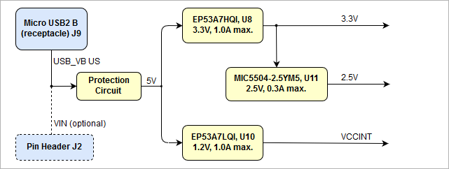
There is no specific or special power-on sequence, just one single power source is needed.
Power Rails
| Connector Designator | VCC / VCCIO Schematic Name | Voltage | Direction | Pins | Notes |
|---|---|---|---|---|---|
| J2 | 5V | 5.0V | Out | Pin 14 | - |
| VIN | 5.0V | In | Pin 13 | - | |
| 3.3V | 3.3V | Out | Pin 12 | - | |
| J6 | 3.3V | 3.3V | Out | Pin 6, 12 | - |
| J9 | USB_VBUS | 5.0V | In | Pin 1 | - |
Table 13: Connector power pin description
Bank Voltages
Bank | Voltage | Voltage Range |
|---|---|---|
| 1 | 3.3V | all bank voltages fixed |
| 2 | 3.3V | |
| 3 | 3.3V | |
| 4 | 3.3V | |
| 5 | 3.3V | |
| 6 | 3.3V | |
| 7 | 3.3V | |
| 8 | 3.3V |
Table 14: FPGA SoC VCCO bank voltages
...
Parameter | Min | Max | Units | Reference document |
|---|---|---|---|---|
VIN supply voltage (5.0V nominal) | -0.3 | 6.0 | V | EP53A7HQI / EP53A7LQI datasheet |
| I/O Input voltage for FPGA I/O bank | -0.35 | 34.632 | V | Intel Cyclone 10 LP datasheet |
Storage Temperature | -40 | +90 | °C | LED R6C-AL1M2VY/3T datasheet |
Table 1315: Absolute maximum ratings
...
| Parameter | Min | Max | Units | Reference document |
|---|---|---|---|---|
| VIN supply voltage (5.0V nominal) | 4.75 | 5.25 | V | same as USB-VBUS specification |
| I/O Input voltage for FPGA I/O bank | 0–0.5 | 3.456 | V | Intel Cyclone 10 LP datasheet |
| Operating temperature range | 0 | +70 | °C | Winbond datasheet W9864G6GT |
Table 1416: Recommended operating conditions
| Note |
|---|
| Please check Intel Cyclone 10 LP datasheet for complete list of absolute maximum and recommended operating ratings for the FPGA device. |
...
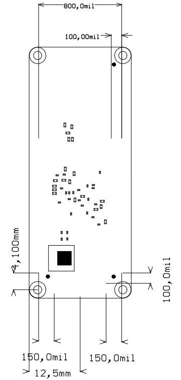
Board size: PCB 25mm × 61,5mm. Notice that some parts the are hanging slightly over the edge of the PCB like the the Micro USB2 B connector, which determine the total physical dimensions of the carrier board. Please download the assembly diagram for exact numbers.
PCB thickness: ca. 1.65mm
Highest part on the PCB without fitted headers and connectors is the Micro USB2 B connector, which has an approximately hight of 3 mm. Please download the step model for exact numbers.
Figure 4
| Scroll Title | ||||
|---|---|---|---|---|
| ||||
|
Revision History
Hardware Revision History
| Date | Revision | Notes | PCN | Documentation Link |
|---|---|---|---|---|
| - | 02 | Second First Production Release | - | TEI0003-02 |
| - | 01 | First Production ReleasePrototypes | - | TEI0003-01 |
Table 1217: Module hardware revision history
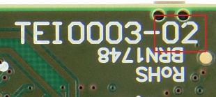
Hardware revision number is printed on the PCB board together with the module model number separated by the dash.
| Scroll Title | ||||
|---|---|---|---|---|
| ||||
Document Change History
| Date | Revision | Contributors | Description | ||||||||||||||||||||||||||||
|---|---|---|---|---|---|---|---|---|---|---|---|---|---|---|---|---|---|---|---|---|---|---|---|---|---|---|---|---|---|---|---|
|
|
|
|
Table 1318: Document change history
Disclaimer
...


