Page History
...
The Trenz Electronic TEI0003 is a low cost small-sized FPGA module integrating a Intel Cyclone 10LP 10CL025 FPGA SoC and , 2 MByte serial memory for configuration and operation, 8 MByte SDRAM and a 3-axis accelerometer.
| HTML |
|---|
<!-- Use short link the Wiki Ressource page: for example: http://trenz.org/te0720-info List of available short links: https://wiki.trenz-electronic.de/display/CON/Redirects --> |
...
Intel Cyclone 10LP 10CL025 FPGA SoC
- 8 MByte SDRAM
2 MByte serial configuration memory
- ST Microelectronics LIS3DH MEMS digital output motion sensor3-axis accelerometer
- JTAG and UART over Micro USB2 connector
- 1x6 pin header for JTAG access to FPGA SoC
- 1x PMOD header providing 8 GPIOs
2x 14-pin headers (2,54 mm pitch) providing 23 GPIOs
- 1x 3-pin header providing 2 GPIOs
8x user LEDs
- 1x user push button
- 35.3V 0V single power supply with on-board voltage regulators
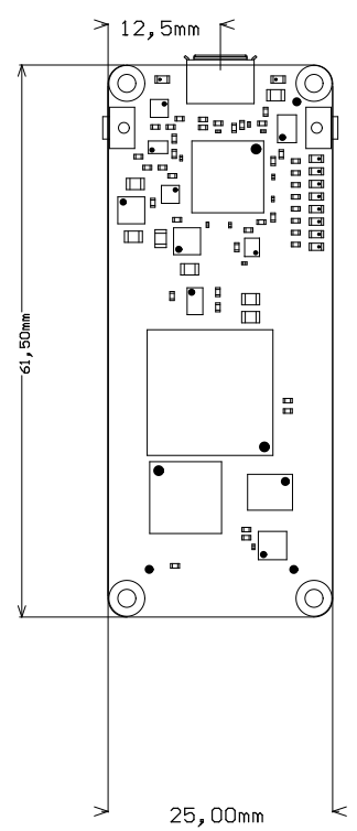
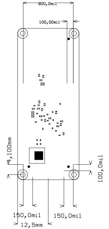
- Size: 61.5 x 25 mm
...
- Intel Cyclone 10LP 10CL025 FPGA SoC, U1
- Winbond W9864G6JT-6 8 Mbyte SDRAM 166MHz, U2
- Intel EPCQ16ASI8N 2 MByte serial configuration memory, U5
- ST Microelectronics LIS3DH MEMS digital output motion sensorLIS3DH 3-axis accelerometer, U4
- FTDI USB2 to JTAG/UART adapter, U3
- Configuration EEPROM for FTDI chip, U9
- 12.0000 MHz oscillator, U7
- 8x red user LEDs, D2 ... D9
- Red LED (Conf. DONE), D10
- Green LED (indicating supply voltage), D1
- Switch Push button (user), S2
- Switch Push button (reset), S1
- Micro USB2 B socket (receptacle), J9
- 1x14 pin header (2.54mm pitch), J2
- 1x6 pin header (2.54mm pitch), J4
- 2x6 Pmod connector, J6
- 3-pin header (2.54mm pitch), J3
- 1x14 pin header (2.54mm pitch), J1
...
By default the configuration mode pins of the FPGA are set to load the FPGA design from the serial configuration memory , hence the FPGA is configured from serial configuration memory at system start-up. The JTAG interface of the module is provided for storing the initial FPGA configuration data to the serial configuration memory.
...
| Bank | Connector Designator | I/O Signal Count | Bank Voltage | Notes |
|---|---|---|---|---|
| 2 | J2 | 9 I/O's | 3.3V | 2 I/O's of bank 2 can be pulled-up to 3.3V (4K7 resistors) with 2 I/O's of same Bank bank or pins can be shared |
| 4 | J1 | 8 I/O's | 3.3V | - |
| J3 | 2 I/O's | 3.3V | - | |
| 5 | J1 | 6 I/O's | 3.3V | - |
| 6 | J6 | 8 I/O's | 3.3V | Pmod Connector |
| 1 | J4 | 4 I/O's | 3.3V | JTAG interface |
| J2 | 1 I/O'sInput | 3.3V | low active Reset input |
Table 2: General overview of single ended I/O signals connected to pin headers and connectors
FPGA I/O banks
| Bank | VCCIO | I/O's Count | Available on ConnectorsConnected to | Notes |
|---|---|---|---|---|
| 1 | 3.3V | 14 | 5 | 6 I/O's connected to FTDI chip, 1 I/O used for user button S2, 2 I/O's connected to red user LEDs D2 and D10. |
| 2 | 3.3V | 37 | 26 | 6 I/O's user for QSPI Flash, 5 I/O's connected to red user LEDs D3 ... D7. |
| 3 | 3.3V | 5 | 5 | Bank 3 is dedicated to JTAG interface. |
| 4 | 3.3V | 24 | 0 | 2 I/O's are dedicated to live probes, all other I/O's are used as memory interface. | 5 |
| 6 | LIS3DH digital motion sensor, U4 | SPI interface, 2 interrupt lines | ||
| 4 | 1x6 pin header, J4 | JTAG interface | ||
| 4 | 2 MByte serial configuration memory, U5 | FPGA configuration memory with active serial (AS) x1 interface | ||
| 1 | J2-10, push button S1 | low active reset input | ||
| 2 | 9 | 1x14 pin header, J2 | GPIOs (2 I/O's of bank 2 can be pulled-up to 3.3V (4K7 resistors) with 2 I/O's of same Bank or pins can be shared) | |
| 3 | 8 | LEDs D2 ... D9 | 8 x red user LEDs | |
| 8 | FTDI FT2232H JTAG/UART Adapter, U3 | configurable as GPIO/UART or other serial interfaces | ||
| 1 | push button S2 | user button | ||
| 4 | 10 | pin headers J1, J3 | GPIOs | |
| 5 | 6 | pin headers J1 | GPIOs | |
| 6 | 8 | Pmod connector J6 | GPIOs | |
| 1 | Red LED, D10 | Configuration DONE Led (ON when configuration in progress, OFF when configuration is done) | ||
| 7 | 19 | 8 Mbyte SDRAM 166MHz, U2 | 16bit SD-RAM memory interface | |
| 8 | 21 | |||
| 6 | 3.3V | 22 | 2 | 2 I/O's available on header J2, 2 I/O's connected to red user LEDs D8 and D9, all other I/O's are used as memory interface. |
| 7 | 8 |
Table 3: General overview of FPGA I/O banks
...
Primary JTAG access to the FPGA SoC device U5 U1 is provided through Micro USB2 B connector J9. The JTAG interface is created by the FTDI FT2232H USB2 to JTAG/UART adapter IC U3.
...
| JTAG Signal | Pin on Header J4 | Note |
|---|---|---|
| TCK | 3 | - |
| TDI | 5 | - |
| TDO | 4 | - |
| TMS | 6 | - |
| JTAGSEL | 2 | The JTAGSEL pin of SmartFusion2 device depends on the used JTAG programmer. |
Table Table 4: optional second JTAG interface or GPIO (JTAGSEL dependent)
QSPI Interface
The QSPI interface of the FPGA device is routed to and used by the on-module QSPI flash IC U1:
...
JTAG pin header
On-board Peripherals
Serial Configuration Memory
On-board serial configuration memory (U5) is provided by Intel EPCQ16ASI8N (EPCQ16SI8N in board revision TEI0003-02A) with 16 MBit (2 MByte) storage capacity. This non volatile memory is used to store initial FPGA configuration via JTAG interface. The memory is connected to FPGA bank 1 via active serial (AS) x1 interface.
| Serial Memory U5 Pin | Signal Schematic Name | Connected to | Notes |
|---|---|---|---|
| Pin 2, DATA1 | AS_DATA0 | FPGA bank 1, pin H2 | Data out |
| Pin 5, DATA0 | AS_ASDO | FPGA bank 1, pin C1 | Data in |
| Pin 1, nCS | AS_NCS | FPGA bank 1, pin D2 | chip select |
| Pin 6, DCLK | AS_DCLK | FPGA bank 1, pin H1 | clock |
Table 5: Serial configuration memory interface connections
SDRAM
The FPGA module is equipped with a Winbond W9864G6JT 64 MBit (8 MByte) SDRAM chip U2. This SDRAM chip is connected to the FPGA bank 7 and 8
Table 5: QSPI interface signals
On-board Peripherals
Quad SPI Flash Memory
On-module QSPI flash memory (U7) is provided by Winbond Serial Flash Memory W74M64FV with 64 MBit (8 MByte) storage capacity. This non volatile memory is used to store initial FPGA configuration. Besides FPGA configuration, remaining free flash memory can be used for user application and data storage.
SDRAM
The TEM0001 FPGA module is equipped with a Winbond W9864G6JT 64 MBit (8 MByte) SDRAM chip U2. This SDRAM chip is connected to the FPGA bank 4 and 7 via 16-bit memory interface with 166MHz clock frequency and CL3 CAS latency.
FTDI FT2232H IC
The FTDI chip U3 converts signals from USB2.0 to a variety of standard serial and parallel interfaces. Refer to the FTDI data sheet to get information about the capacity of the FT2232H chip.
FTDI FT2232H chip is used in MPPSE mode for JTAG, 6 I/O's of Channel B are routed to the bank 1 of the FPGA SoC and are usable for example as UART interface.
The configuration of FTDI FT2232H chip is pre-programmed on the EEPROM U9.
System Clock Oscillator
The FPGA SoC module has following reference clocking signals provided by on-board oscillators:
...
| SDRAM I/O Signals | Signal Schematic Name | Connected to | Notes |
|---|---|---|---|
| Address inputs | A0 ... A13 | bank 8 | - |
| Bank address inputs | BA0 / BA1 | bank 8 | - |
| Data input/output | DQ0 ... DQ15 | bank 7 | - |
| Data mask | DQM0 ... DQM1 | bank 7 | - |
| Clock | CLK | bank 7 | |
| Control Signals | CS | bank 8 | Chip select |
CKE | bank 8 | Clock enable | |
RAS | bank 8 | Row Address Strobe | |
CAS | bank 8 | Column Address Strobe | |
| WE | bank 8 | Write Enable |
Table 6: 16bit SDRAM memory interface
FTDI FT2232H Chip
The FTDI chip U3 converts signals from USB2.0 to a variety of standard serial and parallel interfaces. Refer to the FTDI data sheet to get information about the capacity of the FT2232H chip.
FTDI FT2232H chip is used in MPPSE mode for JTAG, 2 I/O's of channel A and 6 I/O's of Channel B are routed to FPGA bank 3 of the FPGA SoC and are usable for example as GPIOs, UART or other standard interfaces.
The configuration of FTDI FT2232H chip is pre-programmed on the EEPROM U9.
| FTDI Chip U3 Pin | Signal Schematic Name | Connected to | Notes |
|---|---|---|---|
| Pin 12, ADBUS0 | TCK | FPGA bank 1, pin H3 | JTAG interface |
| Pin 13, ADBUS1 | TDI | FPGA bank 1, pin H4 | |
| Pin 14, ADBUS2 | TDO | FPGA bank 1, pin J4 | |
| Pin 15, ADBUS3 | TMS | FPGA bank 1, pin J5 | |
| Pin 17, ADBUS4 | ADBUS4 | FPGA bank 3, pin M8 | user configurable |
| Pin 20, ADBUS7 | ADBUS7 | FPGA bank 3, pin N8 | user configurable |
| Pin 32, BDBUS0 | BDBUS0 | FPGA bank 3, pin | user configurable |
| Pin 33, BDBUS1 | BDBUS1 | FPGA bank 3, pin | user configurable |
| Pin 34, BDBUS2 | BDBUS2 | FPGA bank 3, pin | user configurable |
| Pin 35, BDBUS3 | BDBUS3 | FPGA bank 3, pin | user configurable |
| Pin 37, BDBUS4 | BDBUS4 | FPGA bank 3, pin | user configurable |
| Pin 38, BDBUS5 | BDBUS5 | FPGA bank 3, pin | user configurable |
Table 7: FTDI chip interfaces and pins
3-Axis Accelerometer
On the TEI0003 FPGA board there is a 3-axis accelerometer present. This accelerometer provided by ST Microelectronics LIS3DH offers many function to detect motion and has also a temperature sensor integrated. It also has a FIFO buffer for storing output data. The sensor is connected to the FPGA through SPI interface and two interrupt lines.
| Accelerometer U4 Pin | Signal Schematic Name | Connected to | Notes |
|---|---|---|---|
| Pin 11, INT1 | SEN_INT1 | FPGA bank 1, pin B1 | Interrupt lines |
| Pin 9, INT2 | SEN_INT2 | FPGA bank 1, pin C2 | |
| Pin 6, SDA/SDI/SDO | SEN_SDI | FPGA bank 1, pin G2 | SPI interface |
| Pin 7, SDO/SA0 | SEN_SDO | FPGA bank 1, pin G1 | |
| Pin 4, SCL/SPC | SEN_SPC | FPGA bank 1, pin F3 | |
| Pin 8, CS | SEN_CS | FPGA bank 1, pin D1 | |
| Pin 13, ADC3 | ADC3 | 5V | Sense 5V input voltage |
Table 8: 3-axis accelerometer interfaces and pins
System Clock Oscillator
The FPGA SoC module has following reference clocking signals provided by on-board oscillators:
| Clock Source | Schematic Name | Frequency | Clock Input Destination |
|---|---|---|---|
| Microchip MEMS Oscillator, U7 | CLK12M | 12.0000 MHz | FTDI FT2232 U3, pin 3; FPGA SoC bank 2, pin M2 |
| optional Microchip MEMS Oscillator, U6 (not fitted) | CLK_X | - | FPGA SoC bank 6, pin E15 |
Table 9: Clock sources overview
On-board LEDs
There are 10 LEDs fitted on the FPGA module board. The LEDs are user configurable to indicate for example any system status.
| LED | Color | Signal Schematic Name | FPGA | Notes |
|---|---|---|---|---|
| D1 | Green | - | - | Indicating 3.3V board supply voltage |
| D2 | Red | 'LED1' | bank 6, pin M6 | user |
| D3 | Red | 'LED2' | bank 6, pin T4 | user |
| D4 | Red | 'LED3' | bank 6, pin T3 | user |
| D5 | Red | 'LED4' | bank 6, pin R3 | user |
| D6 | Red | 'LED5' | bank 6, pin T2 | user |
| D7 | Red | 'LED6' | bank 6, pin R4 | user |
| D8 | Red | 'LED7' | bank 6, pin N5 | user |
| D9 | Red | 'LED8' | bank 6, pin N3 | user |
| D10 | Red | 'CONF_DONE' | bank 6, pin H14 | indication configuration is DONE when LED is off |
Table 10: LEDs of the module
Push Buttons
The FPGA module is equipped with two push buttons S1 and S2:
| Button | Signal Schematic Name | FPGA | Notes |
|---|---|---|---|
| S1 | 'USER_BTN' | bank 3, pin N6 | user configurable |
| S2 | 'RESET' | bank 1, pin H5 | system reset |
Table 11: Push buttons of the module
Connectors
All connectors are are for 100mil headers, all connector locations are in 100mil (2.54mm) grid. The module's PCB provides footprints to mount and solder optional pin headers, if those are not factory-fitted on module.
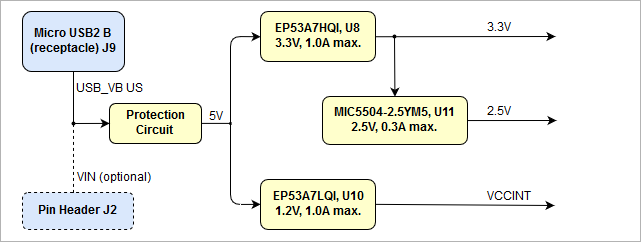
Power and Power-On Sequence
To power-up a module, power supply with minimum current capability of 1A is recommended.
Power Supply
The FPGA module can be power-supplied through Micro USB2 connector J9 with supply voltage 'USB-VBUS' or alternative through pin header J2 with supply voltage 'VIN'.
The TEI0003 module needs one single power supply of 5.0V nominal.
There are following dependencies how the initial voltage of the extern power supply is distributed to the on-board DCDC converters:
| Scroll Title | ||||||||||||||||||||||||||||||
|---|---|---|---|---|---|---|---|---|---|---|---|---|---|---|---|---|---|---|---|---|---|---|---|---|---|---|---|---|---|---|
| ||||||||||||||||||||||||||||||
|
Power Consumption
| FPGA | Design | Typical Power, 25C ambient |
|---|---|---|
| Intel Cyclone 10LP 10CL025 FPGA SoC | Not configured | TBD* |
Table 12: Module power consumption
*TBD - To Be Determined.
Actual power consumption depends on the FPGA design and ambient temperature.
Power-On Sequence
There is no specific or special power-on sequence, just one single power source is needed.
Power Rails
| Connector Designator | VCC / VCCIO Schematic Name | Voltage | Direction | Pins | Notes |
|---|---|---|---|---|---|
| J2 | 5V | 5.0V | Out | Pin 14 | - |
| VIN | 5.0V | In | Pin 13 | - | |
| 3.3V | 3.3V | Out | Pin 12 | - | |
| J6 | 3.3V | 3.3V | Out | Pin 6, 12 | - |
| J9 | USB_VBUS | 5.0V | In | Pin 1 | - |
Table 13: Connector power pin description
Bank Voltages
Bank | Voltage | Voltage Range |
|---|---|---|
| 1 | 3.3V | all bank voltages fixed |
| 2 | 3.3V | |
| 3 | 3.3V | |
| 4 | 3.3V | |
| 5 | 3.3V | |
| 6 | 3.3V | |
| 7 | 3.3V | |
| 8 | 3.3V |
Table 6: Clock sources overview
On-board LEDs
There are 10 LEDs fitted on the FPGA module board. The LEDs are user configurable to indicate for example any system status.
...
Table 7: LEDs of the module
Push Buttons
The TEM0001 FPGA module is equipped with two push buttons S1 and S2:
...
Table 8: Push buttons of the module
Connectors
All connectors are are for 100mil headers, all connector locations are in 100mil (2.54mm) grid. The module's PCB provides footprints to mount and solder optional pin headers, if those are not factory-fitted on module.
Power and Power-On Sequence
To power-up a module, power supply with minimum current capability of 1A is recommended.
Power Supply
The FPGA module can be power-supplied through Micro USB2 connector J9 with supply voltage 'USB-VBUS' or alternative through pin header J2 with supply voltage 'VIN'.
The TEM0001 module needs one single power supply of 5.0V nominal.
There are following dependencies how the initial voltage of the extern power supply is distributed to the on-board DCDC converters:
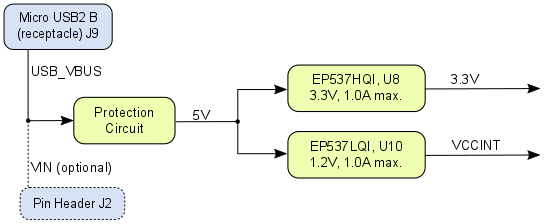
Figure 3: Power Distribution Diagram
Power Consumption
...
Table 9: Module power consumption
*TBD - To Be Determined.
Actual power consumption depends on the FPGA design and ambient temperature.
Power-On Sequence
There is no specific or special power-on sequence, just one single power source is needed.Table 14: FPGA SoC VCCO bank voltages
Technical Specifications
Absolute Maximum Ratings
Parameter | Min | Max | Units | Reference document |
|---|---|---|---|---|
VIN supply voltage (5.0V nominal) | -0.3 | 6.0 | V | EP53A7HQI / EP53A7LQI datasheet |
| I/O Input voltage for FPGA I/O bank | -0.35 | 34.632 | V | Microsemi Intel Cyclone 10 LP datasheet DS0128 |
Storage Temperature | -40 | +90 | °C | LED R6C-AL1M2VY/3T datasheet |
Table 1015: Absolute maximum ratings
...
| Parameter | Min | Max | Units | Reference document |
|---|---|---|---|---|
| VIN supply voltage (5.0V nominal) | 4.75 | 5.25 | V | same as USB-VBUS specification |
| I/O Input voltage for FPGA I/O bank | 0–0.5 | 3.456 | V | Microsemi Intel Cyclone 10 LP datasheetDS0128 |
| Operating temperature range | 0 | +70 | °C | Winbond datasheet W9864G6GT |
Table 1116: Recommended operating conditions
| Note |
|---|
| Please check Microsemi Intel Cyclone 10 LP datasheet DS0128 for complete list of absolute maximum and recommended operating ratings for the FPGA device. |
...
Board size: PCB 25mm × 61,5mm. Notice that some parts the are hanging slightly over the edge of the PCB like the the Micro USB2 B connector, which determine the total physical dimensions of the carrier board. Please download the assembly diagram for exact numbers.
PCB thickness: ca. 1.65mm
Highest part on the PCB without fitted headers and connectors is the Micro USB2 B connector, which has an approximately hight of 3 mm. Please download the step model for exact numbers.
...
| Scroll Title | ||||
|---|---|---|---|---|
| ||||
|
Revision History
Hardware Revision History
| Date | Revision | Notes | PCN | Documentation Link |
|---|---|---|---|---|
| - | 0102 | First Production Release | - | TEI0003-02 TEM0001 |
| - | 01 | Prototypes | - | - |
Table 1217: Module hardware revision history
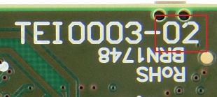
Hardware revision number is printed on the PCB board together with the module model number separated by the dash.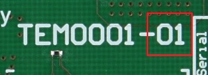
| Scroll Title | ||||
|---|---|---|---|---|
| ||||
|
Document Change History
| Date | Revision | Contributors | Description | ||||||||||||||||||||||||||||
|---|---|---|---|---|---|---|---|---|---|---|---|---|---|---|---|---|---|---|---|---|---|---|---|---|---|---|---|---|---|---|---|
|
|
|
|
Table 1318: Document change history
Disclaimer
...
Overview
Content Tools