Page History
...
Figure 1: TE0725LP-01 Block Diagram.
Main Components
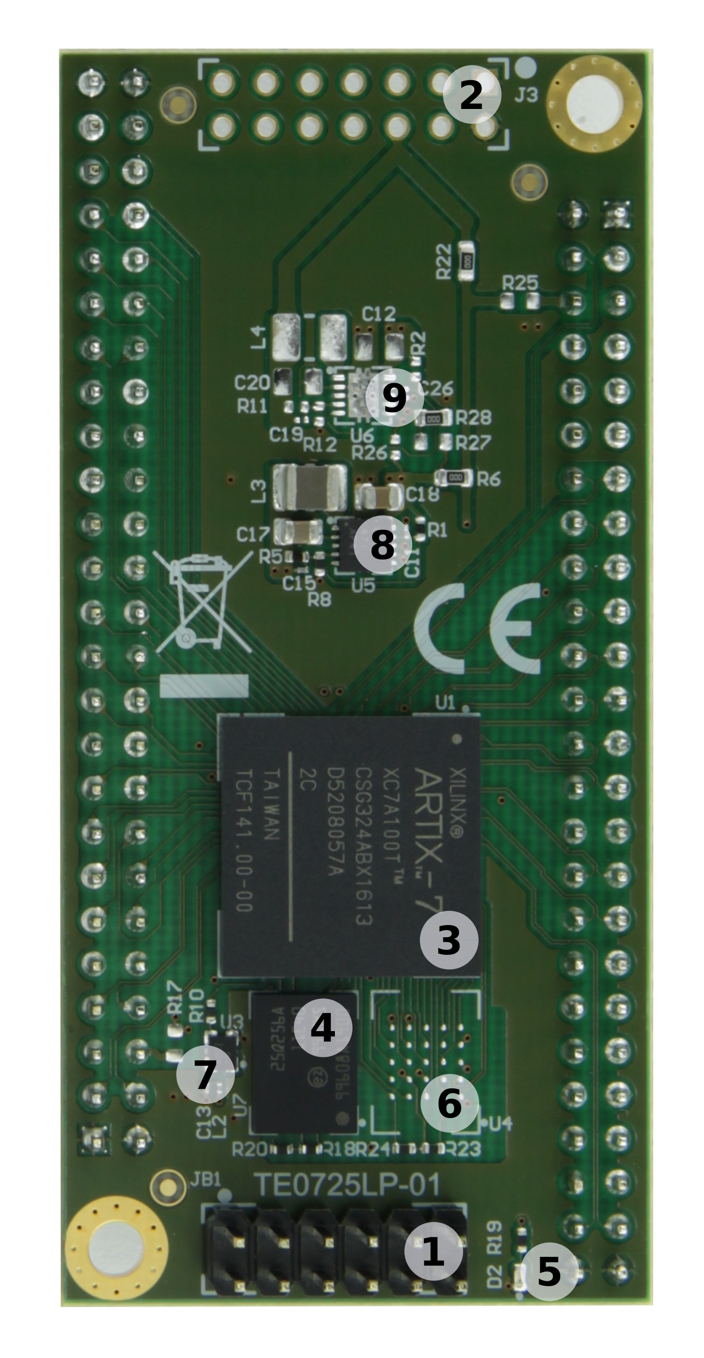
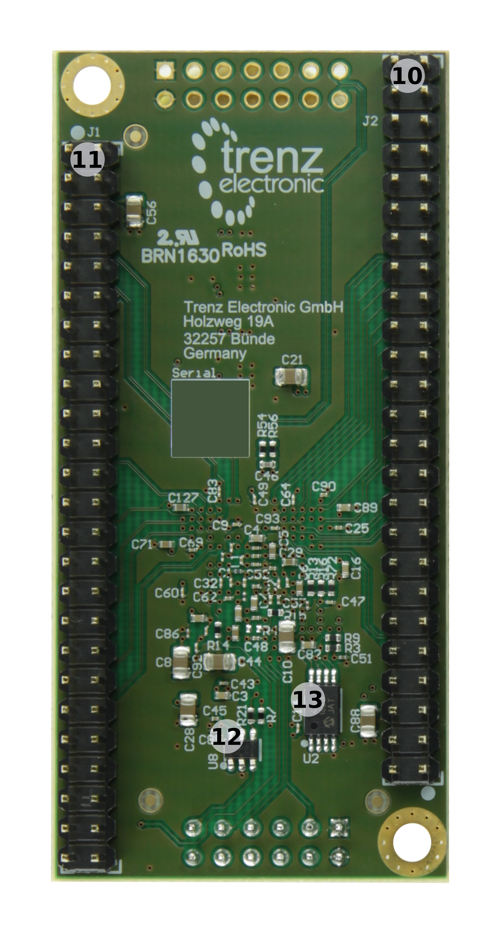
Figure 2: TE0725LP-01 FPGA module (Variant TE0725LP-01-100-2D depicted).
...
A low-power SiTime programmable oscillator (U3) @25.000000 MHz configured on-module @25.000000 MHz is connected to PL I/O-bank 14 and provides the system reference clock signal for the FPGA PL.
On-board LEDs
There is one red LED connected to the FPGA bank 14, pin M16. This LED is user configurable to indicate for example any system status.
...
Parameter | Min | Max | Units | Reference document |
|---|---|---|---|---|
3.3V supply voltage | -0.1 | 3.6 | V | - |
| HR I/O banks supply voltage (VCCO) | -0.5 | 3.6 | V | Xilinx datasheet DS181 |
| HR I/O banks input voltage | -0.4 | VCCO + 0.55 | V | Xilinx datasheet DS181 |
Storage Temperature | -40 | +85 | °C | - |
Table x: General overview of PL I/O signals connected to the B2B connectors.
Recommended Operating Conditions
| ParameterParameter | Min | Max | Units | Reference document |
|---|---|---|---|---|
| VIN supply voltage | 3.135 | 3.45 | V | - |
| HR I/O banks supply voltage (VCCO) | 1.14 | 3.465 | V | Xilinx datasheet DS181 |
| HR I/O banks input voltage | -0.20 | VCCO + 0.20 | V | Xilinx datasheet DS181 |
| Operating Temperature | 0 | +85 | °C | - |
Table x: General overview of PL I/O signals connected to the B2B connectors.
...
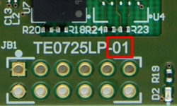
Hardware revision number is printed on the PCB board together with the module model number separated by the dash.
Document Change History
| Date | Revision | Contributors | Description | ||||||||
|---|---|---|---|---|---|---|---|---|---|---|---|
| Jan Kumann | Initial version. |
...
Overview
Content Tools