Page History
...
| HTML |
|---|
<!-- Template Revision 1.63 (HTML comment will not display, it's not needed to remove them. For Template/Skeleton changes, increase Template Revision number. So we can check faster, if the TRM style is up to date) --> |
| Scroll Ignore |
|---|
Download PDF version of this document. |
| Scroll pdf ignore | |
|---|---|
Table of Contents
|
...
| Scroll Only (inline) |
|---|
Refer to https://wiki.trenz-electronic.de/display/PD/TE0725LP+TRM for online version of this manual and the rest of available documentation of the product.
|
The Trenz Electronic TE0725LP is a low cost small-sized FPGA module integrating a Xilinx Artix-7 and 32 MByte Flash memory for configuration and operation.
...
| Bank | Type | B2B Connector | I/O Signal Count | Bank Voltage |
|---|---|---|---|---|
| 14 | HR | J3 | 8 I/O's, 4 LVDS pairs | 1.8V |
| 34 | HR | J2 | 42 I/Os, 21 LVDS pairs | VCCIO34 |
| 35 | HR | J1 | 42 I/Os, 21 LVDS pairs | VCCIO35 |
Table x2: General overview of PL I/O signals connected to the B2B connectors.
...
| Bank | VCCIO | I/O's Count | Available On Connectors | Notes |
|---|---|---|---|---|
| 0 | 3.3V | 7 | 4 | 4 I/O's used for JTAG interface, 3 control signals (DONE, PROG_B, INIT). |
| 14 | 3.3V | 12 | 11 | 8 I/O's (4 LVDS pairs) connected to J3, 3 I/O's to XMOD header JB1 (2 UART I/O's, 1 user I/O), 1 I/O to LED D2. |
| 15 | 1.8V | 18 | 0 | Used for optional HyperFlash™ U4. |
| 34 | User select | 42 | 42 | 0-Ohm resistor R17 option to select 1.8V I/O-bank VCCIO. |
| 35 | User select | 42 | 42 | 0-Ohm resistor R25 option to select 1.8V I/O-bank VCCIO. |
Table x3: General overview of PL I/O-bank signals.
...
| Pin Schematic Name | XMOD Header JB1 Pin | Note |
|---|---|---|
| F_TCK | C (pin J3-4) | - |
| F_TDO | D (pin J3-8) | - |
| F_TDI | F (pin J3-10) | - |
| F_TMS | H (pin J3-12) | - |
| UART_RXD | A (pin J3-3) | UART receive line, connected to PL I/O-bank 14. |
| UART_TXD | B (pin J3-7) | UART transmit line, connected to PL I/O-bank 14. |
| XMOD_E | E (pin J3-9) | User configurable, connected to PL I/O-bank 14, pin M17. |
| NRST | G (pin J3-11) | Assigned to 'PROG_B' (configuration-reset signal of FPGA) via IC U8. |
Table 64: XMOD header JX1 signals and connections.
...
| XMOD DIP-switches | Position |
|---|---|
| Switch 1 | ON |
| Switch 2 | OFF |
| Switch 3 | OFF |
| Switch 4 | ON |
Table 75: XMOD adapter board DIP-switch positions for voltage configuration.
...
| UART Signal Schematic Name | B2B | XMOD Header JX1 | Pin Header J3 | Note |
|---|---|---|---|---|
| B14_L0 | JM2-99 | JX1-7 | J3-7 | UART-TX (transmit line) |
| B14_L25 | JM2-97 | JX1-3 | J3-3 | UART-RX (receive line) |
Table 106: UART interface signals.
QSPI Interface
...
| SD IO Signal Schematic Name | FPGA I/O | Flash IC Memory (U7) Pin | Note |
|---|---|---|---|
| SPI-DQO | Bank 14, pin K17 | D3 | QSPI data |
| SPI-DQ1 | Bank 14, pin K18 | D2 | QSPI data |
| SPI-DQ2 | Bank 14, pin L14 | C4 | QSPI data |
| SPI-DQ3 | Bank 14, pin M14 | D4 | QSPI data |
| SPI_SCK | Bank 0, pin E9 | B2 | QSPI clock |
| SPI-CS | Bank 14, pin L13 | C2 | QSPI chip select |
Table 117: QSPI interface signals.
I2C Interface
...
| I²C Signal Schematic Name | FPGA I/O | EEPROM IC (U2) Pin | Notes |
|---|---|---|---|
| I2C_SDA | Bank 14, pin U18 | 5 | I²C data line, 1.8V reference voltage |
| I2C_SCL | Bank 14, pin U17 | 6 | I²C clock line, 1.8V reference voltage |
| I2C_WP | Bank 14, pin T18 | 7 | Write-protect signal of EEPROM |
Table 108: I2C interface signals.
Differential Analog Input
...
| I²C Signal Schematic Name | FPGA I/O | Connector J3 pinPin | Notes |
|---|---|---|---|
| XADC_P | Bank 0, pin J10 (VP_0) | J3-14 | - |
| XADC_N | Bank 0, pin K9 (VN_0) | J3-13 | - |
Table 109: XADC interface signals.
On-board Peripherals
...
| LED | Color | Signal Schematic Name | FPGA | Notes |
|---|---|---|---|---|
| D2 | Red | 'SYSLED' | Pin M16 | - |
Table x10: LEDs of the module.
Connectors
...
TE0725LP needs one single power supply with nominal of 3.3V .
Power Consumption
at the variant TE0725-01-100-2C or 1.8V at the variants TE0725LP-01-100-2D and TE0725LP-01-100-2D. Following diagram shows the dependencies of the power supply:
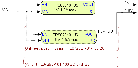
Figure 3: Module power supply dependencies
Power Consumption
| FPGA | Design | FPGA | Design | Typical Power, 25C ambient |
|---|---|---|---|---|
| A100T | Not configured | TBD* |
Table x: General overview of PL I/O signals connected to the B2B connectors.11: Module power consumption
*TBD - To Be Determined.
Actual power consumption depends on the FPGA design and ambient temperature.
...
There is no specific or special power-on sequence, single power source is needed as VIN, rest of the sequence is automatic.
Variants Currently In Production
| Module Variant | FPGA Chip Model | PL Clock | VIN Supply Voltage | HyperFlash™ Memory (U4) | DC-DC TPS62510 (U6) | 2x25 Pin Header J1 | 2x25 Pin Header J2VIN Supply Voltage |
|---|---|---|---|---|---|---|---|
| TE0725LP-01-100-2C | XC7A100T-2CSG324C25 MHz | 3.3 V | fitted | fitted | not fitted | not fitted | |
| TE0725LP-01-100-2D | XC7A100T-2CSG324C | 25 MHz | 1.8 V | not fitted | not fitted | fitted | fitted |
| TE0725LP-01-100-2L | XC7A100T-2CSG324C25 MHz | 1.8 V | not fitted | not fitted | not fitted | not fitted |
Table x: General overview of PL I/O signals connected to the B2B connectors.12: Module variants production
Technical Specifications
Absolute Maximum Ratings
Parameter | Min | Max | Units | Reference document |
|---|---|---|---|---|
3.3V supply voltage | -0.1 | 3.6 | V | - |
| HR I/O banks supply voltage (VCCO) | -0.5 | 3.6 | V | Xilinx datasheet DS181 |
| HR I/O banks input voltage | -0.4 | VCCO + 0.55 | V | Xilinx datasheet DS181 |
Storage Temperature | -40 | +85 | °C | - |
Table x: General overview of PL I/O signals connected to the B2B connectors.13: Absolute maximum ratings
Recommended Operating Conditions
| Parameter | Min | Max | Units | Reference document |
|---|---|---|---|---|
| VIN supply voltage | 3.135 | 3.45 | V | - |
| HR I/O banks supply voltage (VCCO) | 1.14 | 3.465 | V | Xilinx datasheet DS181 |
| HR I/O banks input voltage | -0.20 | VCCO + 0.20 | V | Xilinx datasheet DS181 |
| Operating Temperature | 0 | +85 | °C | - |
Table x: General overview of PL I/O signals connected to the B2B connectors.14: Recommended operating conditions
| Note |
|---|
| Please check Xilinx datasheet DS181 for complete list of absolute maximum and recommended operating ratings for the Artix-7 device. |
...
All 100 mil pin headers are in 100 mil grid, the M3 mounting holes are in 50 mil grid aligned to the centers of the 100mil headers. The module is symmetrical, turning it 180 degrees will keep all I/O and Power pins in both 50 pin headers in compatible places.headers in compatible places.
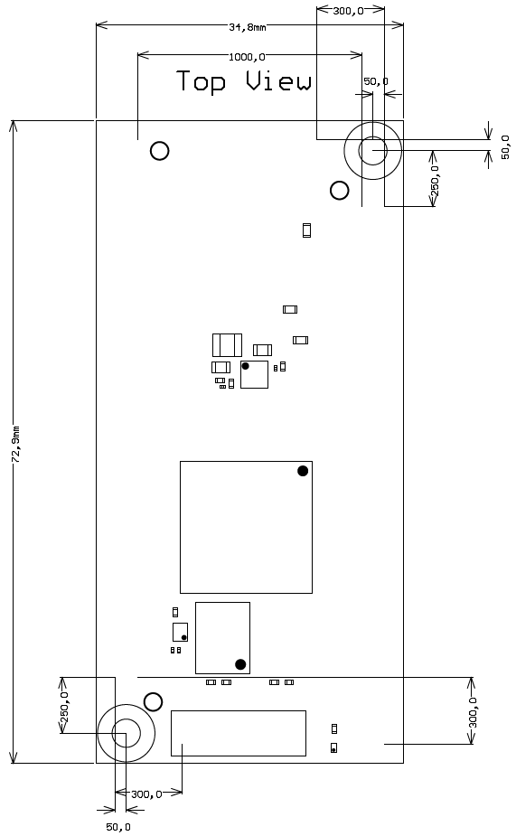
Figure 4: Module physical dimensions drawing
Operating Temperature Ranges
...
| Date | Revision | Notes | PCN | Documentation Link |
|---|---|---|---|---|
| 2016-07-21 | 01 | Prototypes |
Table x:15: Module hardware revision historyGeneral overview of PL I/O signals connected to the B2B connectors.
Hardware revision number is printed on the PCB board together with the module model number separated by the dash.
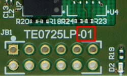
Figure 5: Module hardware revision number
Document Change History
| Date | Revision | Contributors | Description | ||||||||
|---|---|---|---|---|---|---|---|---|---|---|---|
| Jan Kumann | Initial version. |
Table x: General overview of PL I/O signals connected to the B2B connectors.16: Document change history
Disclaimer
| Include Page | ||||
|---|---|---|---|---|
|
Overview
Content Tools