Page History
...
| HTML |
|---|
<!-- Template Revision 1.63 (HTML comment will not display, it's not needed to remove them. For Template/Skeleton changes, increase Template Revision number. So we can check faster, if the TRM style is up to date) --> |
| scroll-ignore | |
|---|---|
| scroll-pdf-ignore | |
Table of Contents
|
...
There is no specific or special power-on sequence, single power source is needed as VIN.
Variants Currently In Production
Voltage Monitor Circuit
The 1.8V voltage level is monitored by the voltage monitor circuit U8, which generates the PROG_B signal to begin a new configuration sequence after reset of the FPGA. A manual reset is also possible by driving the connector pin JB1-11 ('NRST') to GND. Hence, by this pin a mounted XMOD adapter board can perform a reset on the FPGA module.
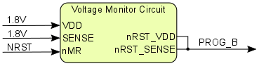
Figure 4: Voltage monitor circuit
Power Rails
Power Rail Name | J1 Pins | J2 Pins | J3 Pins | JB1 Pin | Direction | Notes |
|---|---|---|---|---|---|---|
| VIN | 5 | 5 | 5 | - | Input | Power supply voltage |
| 1.8V | - | - | - | 6 | Output | JTAG VCCIO |
| 1.8V_OUT | - | - | - | 6 | Output | - |
| VCCIO34 | - | 6, 45 | - | - | Input | Bank voltage |
| VCCIO35 | 6, 45 | - | - | - | Input | Bank voltage |
Table 13: Board power rails
Bank Voltages
Bank | Bank I/O Voltage VCCO | Voltage Range |
|---|---|---|
| 0 (config) | 1.8V | fixed |
| 14 (HR) | 1.8V | fixed |
| 15 (HR) | 1.8V | fixed |
| 34 (HR) | VCCIO34 | 1.2V ... 3.3V |
| 35 (HR) | VCCIO34 | 1.2V ... 3.3V |
Table 14: Board bank voltages
Variants Currently In Production
| Module Variant | FPGA Chip Model | Module Variant | FPGA Chip Model | HyperFlash™ Memory (U4) | DC-DC TPS62510 (U6) | 2x25 Pin Header J1 | 2x25 Pin Header J2 |
|---|---|---|---|---|---|---|---|
| TE0725LP-01-100-2C | XC7A100T-2CSG324C | fitted | fitted | not fitted | not fitted | ||
| TE0725LP-01-100-2D | XC7A100T-2CSG324C | not fitted | not fitted | fitted | fitted | ||
| TE0725LP-01-100-2L | XC7A100T-2CSG324C | not fitted | not fitted | not fitted | not fitted |
...
The dimensions are given in mm and mil (milli inch).
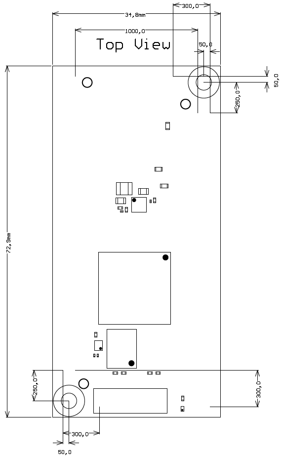
Figure 45: Module physical dimensions drawing
...
Hardware revision number is printed on the PCB board together with the module model number separated by the dash.
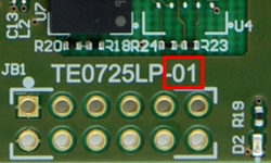
Figure 56: Module hardware revision number
...
Overview
Content Tools