Page History
| HTML |
|---|
<!--
Template Revision 1.5
--> |
| Scroll Only (inline) |
|---|
Online version of this manual and other related documents can be found at https://wiki.trenz-electronic.de/display/PD/SC-CPLD-Firmware |
| Scroll pdf ignore | ||||
|---|---|---|---|---|
Table of contents
|
...
...
...
...
...
...
...
...
...
...
...
...
...
...
...
...
...
...
...
...
...
...
...
...
...
...
...
...
...
...
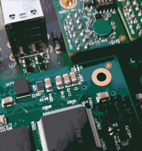
Green LED D2
...
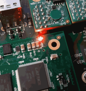
Red LED D1
...
RED LED D1 (SYSLED2) shows a certain blinking pattern in case one of the status signals is active, otherwise it can be controlled via I2C from FPGA side or is simply OFF.
| Blink sequence | Priority | Condition | Description | |||||
|---|---|---|---|---|---|---|---|---|
********
| highest | SC_nRST= LOW (low active) | external reset from carrier is pressed | |||||
| *******o | blink sequence not used | |||||||
| ******oo | blink sequence not used | |||||||
| *****ooo | PG_ALL is zero | One of the power rails of the internal Voltages DCDCs is down | ||||||
| ****oooo | EN1 is zero | B2B enable Pin is active (low active), coming from the carrier | ||||||
| ***ooooo | blink sequence not used | |||||||
| **oooooo | blink sequence not used | |||||||
*ooooooo
| DONE = '0' | FPGA not programmed. No design on QSPI Flash? | ||||||
| continuously ON | lowest | software controlled command via I2C Interface. LED = GPIO_output(1) when GPIO_output(0) = 0 | Set bit GPIO_output(0) LOW to control the LED with GPIO_output(1). | |||||
| continuously OFF | If none of the above condition is met |
GREEN LED D2 (SYSLED1) software controlled command via I2C Interface or is simply OFF.
| Blink sequence | Condition | Description |
|---|---|---|
| continuously ON | software controlled command via I2C Interface. LED = GPIO_output(3) when GPIO_output(2) = 0 | Set bit GPIO_output(2) LOW to control the LED with GPIO_output(3). |
| continuously OFF | If none of the above condition is met |
I2C Interface
This subsystem provides 2 x 32-bit (segmented in eight 8-bit) of general purpose parallel input and output (I/O) expansion for the I2C bus protocol. Address of this I2C device is 0x20. This module contains eight 8-bit registers for reading and writing (GPIO_input[7:0] to GPIO_input[31:24] and GPIO_output[7:0] to GPIO_output[31:24]) separately with address 0x00 to 0x03. These registers can be accessed with I2C commands on a standalone application or, more simply, from petalinux running on the Microblaze. Refer to TE0710 reference design (test board).
| Expand | ||
|---|---|---|
| ||
|
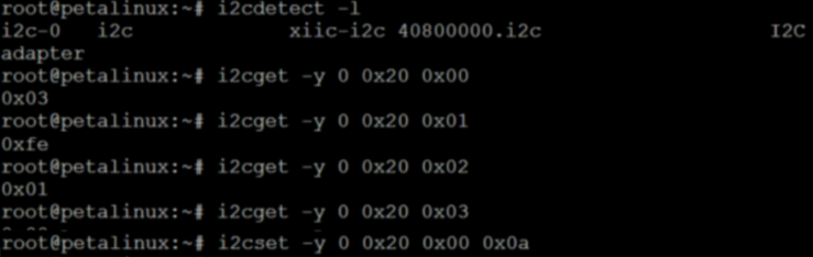
Four registers can be read and four can be written.
| GPIO_input(7 downto 0) | readable | 0x00 | contains the CPLD Firmware Revision (not the PCB revision) |
| GPIO_input(15 downto 8) | readable | 0x01 | SC_nRST, BOOTMODE, PGOOD, EN1, DONE, PG_ALL, NOSEQ, '0' |
| GPIO_input(23 downto 16) | readable | 0x02 | contains: NOSEQ state in bit 16. |
| GPIO_input(31 downto 24) | readable | 0x03 | empty |
| GPIO_output(7 downto 0) | writeable | 0x00 | Bit 1 to 3 are mapped to SYSLED1 and SYSLED2. Write '1' to Bit 1 and Bit 3 to turn on the LED D1 and D2. |
| GPIO_output(15 downto 8) | writeable | 0x01 | not mapped |
| GPIO_output(23 downto 16) | writeable | 0x02 | Bit 16 is mapped to NOSEQ if no reset occurs |
| GPIO_output(31 downto 24) | writeable | 0x03 | not mapped |
...
...
...
...
...
...
...
...
Overview
Content Tools