...
- Modules/ SoC FPGA
- RAM/Storage
- On Board
- 1x 4x Current Sensor
- 1x 4x ADC
- 2x Terminal Blocks
- 2x Power Regulators
- 3x Half-Bridge Drivers
- Interface
- 2x Pmod Pin Header (2x6 Pol)
- Power
- 3.3V supply voltage from Pmods
- Supply current and voltage monitoring
- Dimension
...
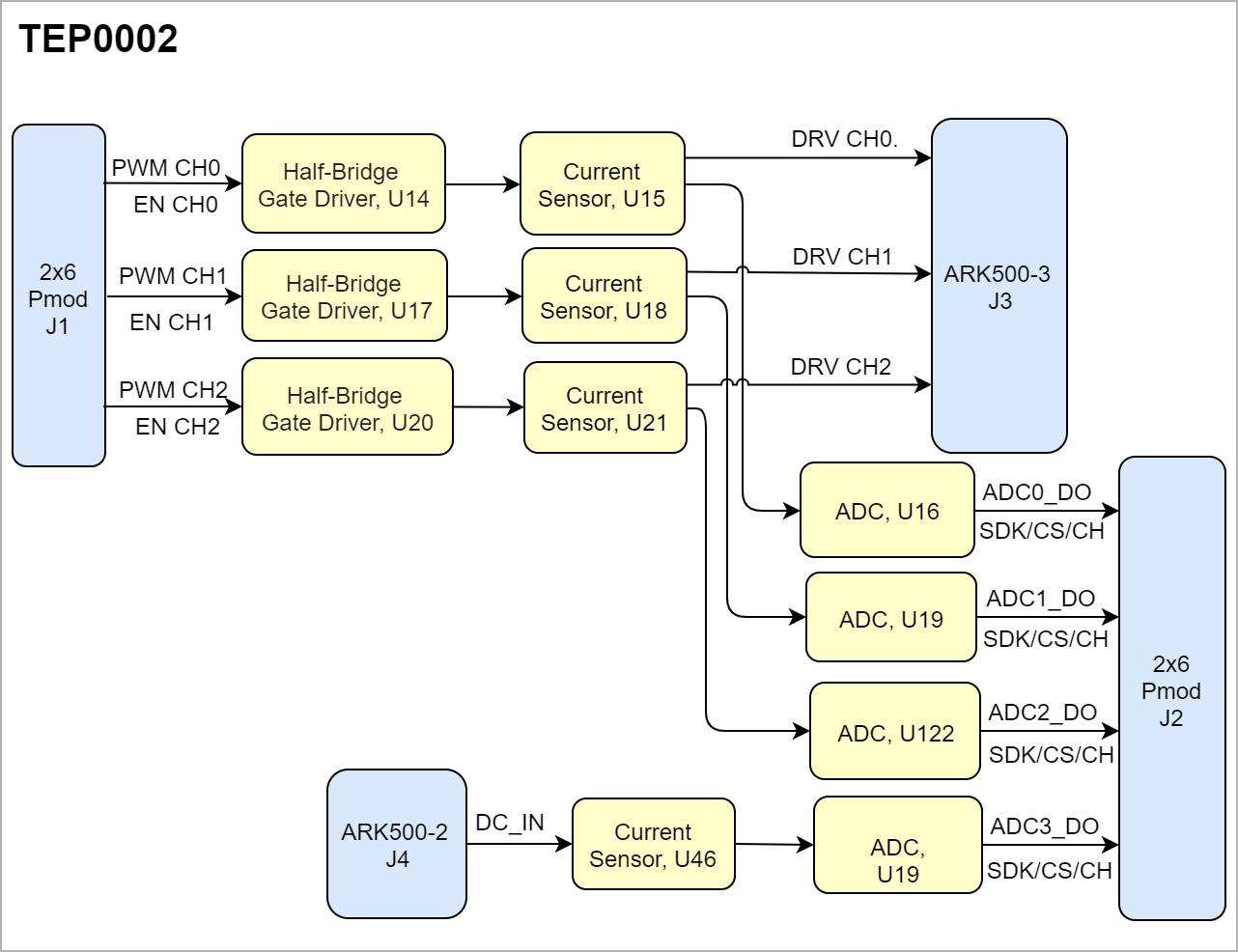
| Scroll Title |
|---|
| anchor | Figure_OV_BD |
|---|
| title | TEP0002 block diagram |
|---|
|
| Scroll Ignore |
|---|
| draw.io Diagram |
|---|
| border | false |
|---|
| viewerToolbar | true |
|---|
| |
|---|
| fitWindow | false |
|---|
| diagramName | TEP0002_block |
|---|
| simpleViewer | false |
|---|
| links | auto |
|---|
| tbstyle | hidden |
|---|
| lbox | true |
|---|
| diagramWidth | 641 |
|---|
| revision | 1116 |
|---|
|
|
| Scroll Only |
|---|
|
|
Main Components
...
| Scroll Title |
|---|
| anchor | Figure_OV_MC |
|---|
| title | TEP0002 main components |
|---|
|
| Scroll Ignore |
|---|
| draw.io Diagram |
|---|
| border | false |
|---|
| viewerToolbar | true |
|---|
| |
|---|
| fitWindow | false |
|---|
| diagramName | TEP0002_MC |
|---|
| simpleViewer | false |
|---|
| links | auto |
|---|
| tbstyle | hidden |
|---|
| lbox | true |
|---|
| diagramWidth | 641 |
|---|
| revision | 57 |
|---|
|
|
| Scroll Only |
|---|
|
|
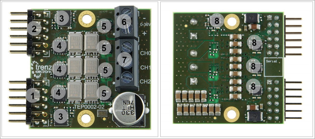
- 2x6 PMod 2x6 Peripheral Header, J2J1
- 2x6 PMod 2x6 Peripheral Header, J1J2
- Power Regulators, U1-U7
- Hall Effect Linear Current SensorHalf Bridge Gate Drivers, U14-U17-U20
- Current Sensors, U15-U18-U21-U46
- ARK500-2 screw connector, J2
- ARK500-3 screw connector, J3
- Analog Digital Converter, U46
J3 connector
...
- U16-U19-U22-U47
Initial Delivery State
| Page properties |
|---|
|
Notes : Only components like EEPROM, |
J4 connector
...
Initial Delivery State
| Page properties |
|---|
|
Notes : Only components like EEPROM, QSPI flash can be initialized by default at manufacture. If there is no components which might have initial data ( possible on carrier) you must keep the table empty |
...
| Scroll Title |
|---|
| anchor | Table_SIP_Pmod |
|---|
| title | General Pmod connectors information |
|---|
|
| Scroll Table Layout |
|---|
| orientation | portrait |
|---|
| sortDirection | ASC |
|---|
| repeatTableHeaders | default |
|---|
| style | |
|---|
| widths | |
|---|
| sortByColumn | 1 |
|---|
| sortEnabled | false |
|---|
| cellHighlighting | true |
|---|
|
| Pin | Pmod J1 | Pmod J2 | Notes |
|---|
| 1 | PWM_CH0 | ADC_CH |
| | 2 | PWM_CH1 | ADC AD_SCK |
| | 3 | PWM_CH2 | ADC_CS |
| | 4 | N.C | Sensor fault |
| | 5 | GND | GND |
| | 6 | VCC | VCC |
| | 7 | EN_CH0 | ADC_DO0 |
| | 8 | EN_CH1 | ADC_DO1 |
| | 9 | EN_CH2 | ADC_DO2 |
| | 10 | N.C | ADC_DO3 |
| | 11 | GND | GND |
| | 12 | VCC | VCC |
|
On-board Peripherals
| Page properties |
|---|
|
Notes : - add subsection for every component which is important for design, for example:
- Two 100 Mbit Ethernet Transciever PHY
- USB PHY
- Programmable Clock Generator
- Oscillators
- eMMCs
- RTC
- FTDI
- ...
- DIP-Switches
- Buttons
- LEDs
|
| Page properties |
|---|
|
Notes : In the on-board peripheral table "chip/Interface" must be linked to the corresponding chapter or subsection |
...
| anchor | Table_OBP |
|---|
| title | On board peripherals |
|---|
Terminal blocks
The TEP0002 is equipped with two Terminal Blocks J3 and J4.
| Scroll Title |
|---|
| anchor | Table_SIP_TerBlk |
|---|
| title | Terminal Blocks information |
|---|
|
| Scroll Table Layout |
|---|
| orientation | portrait |
|---|
| sortDirection | ASC |
|---|
| repeatTableHeaders | default |
|---|
| style | |
|---|
| widths | |
|---|
| sortByColumn | 1 |
|---|
| sortEnabled | false |
|---|
| cellHighlighting | true |
|---|
|
| Designator | Pin | Schematic | Notes |
|---|
| J3 | 1 | DRV_CH2 | ARK500-3 | | 2 | DRV_CH1 | ARK500-3 | | 3 | DRV_CH0 | ARK500-3 | | J4 | 1 | DC_IN | ARK500-2 | | 2 | GND | ARK500-2 |
|
On-board Peripherals
| Page properties |
|---|
|
Notes : - add subsection for every component which is important for design, for example:
- Two 100 Mbit Ethernet Transciever PHY
- USB PHY
- Programmable Clock Generator
- Oscillators
- eMMCs
- RTC
- FTDI
- ...
- DIP-Switches
- Buttons
- LEDs
|
| Page properties |
|---|
|
Notes : In the on-board peripheral table "chip/Interface" must be linked to the corresponding chapter or subsection |
...
RTC
| Scroll Title |
|---|
| anchor | Table_OBP_RTC |
|---|
| title | I2C interface MIOs and pins |
|---|
|
| Scroll Table Layout |
|---|
| orientation | portrait |
|---|
| sortDirection | ASC |
|---|
| repeatTableHeaders | default |
|---|
style | widths | | sortByColumn | 1 |
|---|
| sortEnabled | false |
|---|
| cellHighlighting | true |
|---|
| MIO Pin | Schematic | U? Pin | Notes |
|---|
| Scroll Title |
|---|
| anchor | Table_OBP_I2C_RTC |
|---|
| title | I2C Address for RTCOn board peripherals |
|---|
|
| Scroll Table Layout |
|---|
| orientation | portrait |
|---|
| sortDirection | ASC |
|---|
| repeatTableHeaders | default |
|---|
| style | |
|---|
| widths | |
|---|
| sortByColumn | 1 |
|---|
| sortEnabled | false |
|---|
| cellHighlighting | true |
|---|
|
| MIO Pin | I2C Address| Chip/Interface | Designator | Notes |
|---|
|
LEDs
Analog Digital Converters
The TEP0006 is equipped with four Analog Digital Converters.
| scroll-scroll-title |
|---|
| anchor | Table_OBP_LEDADC |
|---|
| title | On-board LEDsADC Information |
|---|
|
| Scroll Table Layout |
|---|
| orientation | portrait |
|---|
| sortDirection | ASC |
|---|
| repeatTableHeaders | default |
|---|
| style | |
|---|
| widths | |
|---|
| sortByColumn | 1 |
|---|
| sortEnabled | false |
|---|
| cellHighlighting | true |
|---|
|
Designator| Color | Active Level | Note | |
Clock Sources
...
| anchor | Table_OBP_CLK |
|---|
| title | Osillators |
|---|
...
Power and Power-On Sequence
...
In 'Power and Power-on Sequence' section there are three important digrams which must be drawn:
- Power on-sequence
- Power distribution
- Voltage monitoring circuit
| Note |
|---|
For more information regarding how to draw diagram, Please refer to "Diagram Drawing Guidline" . |
Power Supply
Power supply with minimum current capability of xx A for system startup is recommended.
Power Consumption
...
| anchor | Table_PWR_PC |
|---|
| title | Power Consumption |
|---|
...
* TBD - To Be Determined
Power Distribution Dependencies
...
| anchor | Figure_PWR_PD |
|---|
| title | Power Distribution |
|---|
| Scroll Ignore |
|---|
Create DrawIO object here: Attention if you copy from other page, objects are only linked. |
| Scroll Only |
|---|
image link to the generate DrawIO PNG file of this page. This is a workaround until scroll pdf export bug is fixed |
| Notes |
|---|
| ADC,U16 | ADC,U19 | ADC,U22 | ADC,U47 |
|---|
| AVDD | 5AV | 5AV | 5AV | 5AV |
| | REF | Current Sensors,U17 | Current Sensors,U20 | Current Sensors,U22 | Current Sensors,U46 | VCC Pin | | AIN0+ | DRV_CH0 | DRV_CH1 | DRV_CH2 | DC_IN |
| | AIN0- | GND | GND | GND | GND |
| | AIN1+ | Current Sensors,U17 | Current Sensors,U20 | Current Sensors,U22 | Current Sensors,U46 | VIOUT Pin | | AIN1- | GND | GND | GND | GND |
| | REFGND | GND | GND | GND | GND |
| | DVDD | 3.3V | 3.3V | 3.3V | 3.3V |
| | SCLK | ADC_SCK | ADC_SCK | ADC_SCK | ADC_SCK | PMod J2 | | SDO | ADC0_DO | ADC1_DO | ADC2_DO | ADC3_DO | PMod J2 | | nCS | ADC_CS | ADC_CS | ADC_CS | ADC_CS | PMod J2 | | CH_SEL | ADC_CH | ADC_CH | ADC_CH | ADC_CH | PMod J2 | | PDEN | GND | GND | GND | GND |
| | GND | GND | GND | GND | GND |
|
|
Power and Power-On Sequence
| Page properties |
|---|
|
In 'Power and Power-on Sequence' section there are three important digrams which must be drawn: - Power on-sequence
- Power distribution
- Voltage monitoring circuit
|
Power Supply
Power supply with minimum current capability of xx A for system startup is recommended.
Power Consumption
| Scroll Title |
|---|
| anchor | Table_PWR_PC |
|---|
| title | Power Consumption |
|---|
|
| Scroll Table Layout |
|---|
| orientation | portrait |
|---|
| sortDirection | ASC |
|---|
| repeatTableHeaders | default |
|---|
| style | |
|---|
| widths | |
|---|
| sortByColumn | 1 |
|---|
| sortEnabled | false |
|---|
| cellHighlighting | true |
|---|
|
| Power Input Pin | Typical Current |
|---|
| VIN | TBD* |
|
* TBD - To Be Determined
Power Distribution Dependencies
| Scroll Title |
|---|
| anchor | Figure_PWR_PD |
|---|
| title | Power Distribution |
|---|
|
| Scroll Ignore |
|---|
| draw.io Diagram |
|---|
| border | false |
|---|
| viewerToolbar | true |
|---|
| |
|---|
| fitWindow | false |
|---|
| diagramDisplayName | |
|---|
| lbox | true |
|---|
| revision | 5 |
|---|
| diagramName | TEP0002_PWR_PD |
|---|
| simpleViewer | false |
|---|
| width | |
|---|
| links | auto |
|---|
| tbstyle | hidden |
|---|
| diagramWidth | 641 |
|---|
|
|
| Scroll Only |
|---|
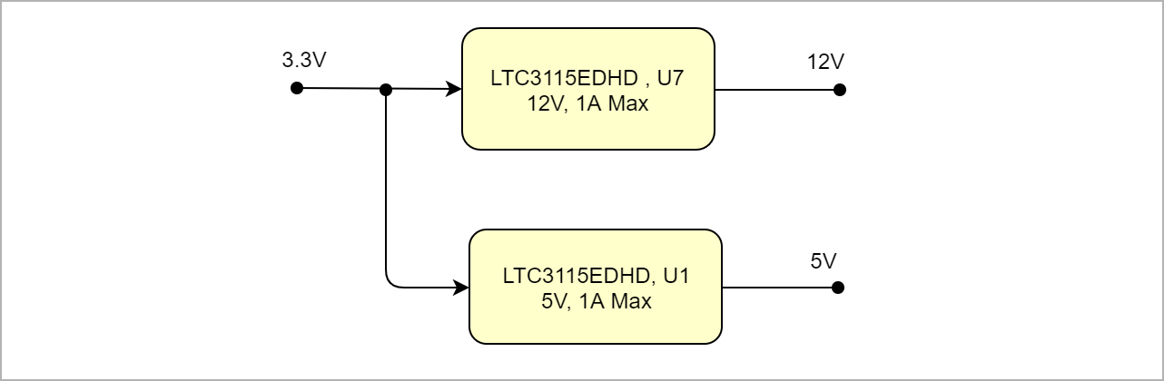 Image Added Image Added
|
|
Power-On Sequence
There is no specific power on sequence, after power on the module all regulators will be enable.
Power Rails
Power-On Sequence
...
| anchor | Figure_PWR_PS |
|---|
| title | Power Sequency |
|---|
| Scroll Ignore |
|---|
Create DrawIO object here: Attention if you copy from other page, objects are only linked. |
| Scroll Only |
|---|
image link to the generate DrawIO PNG file of this page. This is a workaround until scroll pdf export bug is fixed |
Voltage Monitor Circuit
...
| anchor | Figure_PWR_VMC |
|---|
| title | Voltage Monitor Circuit |
|---|
| Scroll Ignore |
|---|
Create DrawIO object here: Attention if you copy from other page, objects are only linked. |
| Scroll Only |
|---|
image link to the generate DrawIO PNG file of this page. This is a workaround until scroll pdf export bug is fixed |
Power Rails
...
| anchor | Table_PWR_PR |
|---|
| title | Module power rails. |
|---|
...
Pmod J1 Pin
...
Pmod J2 Pin
...
Bank Voltages
| Scroll Title |
|---|
| anchor | Table_PWR_BVPR |
|---|
| title | Zynq SoC bank voltagesModule power rails. |
|---|
|
| Scroll Table Layout |
|---|
| orientation | portrait |
|---|
| sortDirection | ASC |
|---|
| repeatTableHeaders | default |
|---|
| style | |
|---|
| widths | |
|---|
| sortByColumn | 1 |
|---|
| sortEnabled | false |
|---|
| cellHighlighting | true |
|---|
|
| Power Rail Name | Pmod J1 Pin | Pmod J2 Pin | Direction | Notes |
|---|
| 3.3V | 6,12 | 6,12 | Input |
| Schematic Name | | Notes
|
Technical Specifications
Absolute Maximum Ratings
| Scroll Title |
|---|
| anchor | Table_TS_AMR |
|---|
| title | PS absolute maximum ratings |
|---|
|
| Scroll Table Layout |
|---|
| orientation | portrait |
|---|
| sortDirection | ASC |
|---|
| repeatTableHeaders | default |
|---|
| style | |
|---|
| widths | |
|---|
| sortByColumn | 1 |
|---|
| sortEnabled | false |
|---|
| cellHighlighting | true |
|---|
|
| Symbols | Description | Min | Max | Unit |
|---|
V | VV | | STG_T | Storage Temperature | -40 | 105 | °C |
V | V | V | V
|
Recommended Operating Conditions
...
| Scroll Title |
|---|
| anchor | Table_TS_ROC |
|---|
| title | Recommended operating conditions. |
|---|
|
| Scroll Table Layout |
|---|
| orientation | portrait |
|---|
| sortDirection | ASC |
|---|
| repeatTableHeaders | default |
|---|
| style | |
|---|
| widths | |
|---|
| sortByColumn | 1 |
|---|
| sortEnabled | false |
|---|
| cellHighlighting | true |
|---|
|
| Parameter | Min | Max | Units | Reference Document |
|---|
| 3.3V | 3.0 | 4.2 | V |
| | OPT_T | -40 | 105 | °C | See ARK500-2 and ARK500-3 Data Sheet | V | See ???? datasheets. | V | See Xilinx ???? datasheet. | °C | See Xilinx ???? datasheet. | °C | See Xilinx ???? datasheet. |
|
Physical Dimensions
Module size: 40 mm × 40 mm. Please download the assembly diagram for exact numbers.
...
| Scroll Title |
|---|
| anchor | Figure_TS_PD |
|---|
| title | Physical Dimension | | Physical Dimension |
|---|
|
| Scroll Ignore |
|---|
| draw.io Diagram |
|---|
| border | false |
|---|
| viewerToolbar | true |
|---|
| |
|---|
| fitWindow | false |
|---|
| diagramDisplayName | |
|---|
| lbox | true |
|---|
| revision | 4 |
|---|
| diagramName | TEP0002_TS_PD |
|---|
| simpleViewer | false |
|---|
| width | |
|---|
| links | auto |
|---|
| tbstyle | hidden |
|---|
| diagramWidth | 641 |
|---|
|
| | Scroll Ignore |
|---|
| Create DrawIO object here: Attention if you copy from other page, objects are only linked. |
| Scroll Only |
|---|
| scroll-pdf | true |
|---|
| scroll-office | true |
|---|
| scroll-chm | true |
|---|
| scroll-docbook | true |
|---|
| scroll-eclipsehelp | true |
|---|
| scroll-epub | true |
|---|
| scroll-html | true |
|---|
| image link to the generate DrawIO PNG file of this page. This is a workaround until scroll pdf export bug is fixed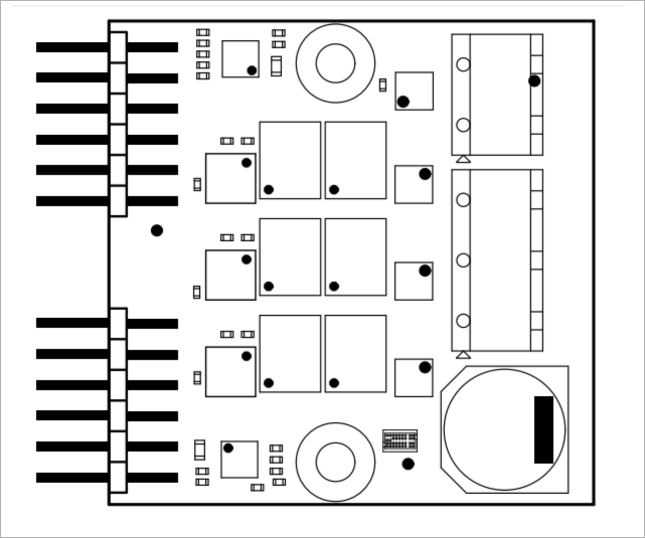 Image Added Image Added |
|
Currently Offered Variants
...
| Scroll Title |
|---|
| anchor | Table_RH_HRH |
|---|
| title | Hardware Revision History |
|---|
|
| Scroll Table Layout |
|---|
| orientation | portrait |
|---|
| sortDirection | ASC |
|---|
| repeatTableHeaders | default |
|---|
| style | |
|---|
| widths | |
|---|
| sortByColumn | 1 |
|---|
| sortEnabled | false |
|---|
| cellHighlighting | true |
|---|
|
| Date | Revision | Changes | Documentation Link |
|---|
| 2019-04-23 | 03 | - R18 and C46 have been removed
- R22 and C57 have been removed
- R26 and C67 have been removed
- R17, R20, R21, R24, R25, R28 have been renamed and the resistance level have been change
- U1 and U7 have been changed to LM4510SD
| REV03 |
| Date | Revision | Changes | Documentation Link |
|---|
2017-03-09 | REV01 | REV012019 | | 2018-02-27 | 02 | - Schematic has been updated
| REV02 |
REV02 | 0423REV03 | REV03
|
Hardware revision number can be found on the PCB board together with the module model number separated by the dash.
| Scroll Title |
|---|
| anchor | Figure_RV_HRN |
|---|
| title | Board hardware revision number. |
|---|
|
| Scroll Ignore |
|---|
| draw.io Diagram |
|---|
| border | false |
|---|
| viewerToolbar | true |
|---|
| |
|---|
| fitWindow | false |
|---|
| diagramDisplayName | |
|---|
| lbox | true |
|---|
| revision | 2 |
|---|
| diagramName | TEP0002_RV_HRN |
|---|
| simpleViewer | false |
|---|
| width | |
|---|
| links | auto |
|---|
| tbstyle | hidden |
|---|
| diagramWidth | 148 |
|---|
|
|
| Scroll Only |
|---|
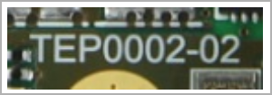 Image Added Image Added
| Create DrawIO object here: Attention if you copy from other page, objects are only linked. | | Scroll Only |
|---|
image link to the generate DrawIO PNG file of this page. This is a workaround until scroll pdf export bug is fixed |
|
Document Change History
| Page properties |
|---|
|
- Note this list must be only updated, if the document is online on public doc!
- It's semi automatically, so do following
Add new row below first Copy "Page Information Macro(date)" Macro-Preview, Metadata Version number, Author Name and description to the empty row. Important Revision number must be the same as the Wiki document revision number Update Metadata = "Page Information Macro (current-version)" Preview+1 and add Author and change description. --> this point is will be deleted on newer pdf export template - Metadata is only used of compatibility of older exports
|
...
| Scroll Title |
|---|
| anchor | Table_RH_DCH |
|---|
| title | Document change history. |
|---|
|
| Scroll Table Layout |
|---|
| orientation | portrait |
|---|
| sortDirection | ASC |
|---|
| repeatTableHeaders | default |
|---|
| style | |
|---|
| widths | |
|---|
| sortByColumn | 1 |
|---|
| sortEnabled | false |
|---|
| cellHighlighting | true |
|---|
|
| Date | Revision | Contributor | Description |
|---|
| Page info |
|---|
| infoType | Modified date |
|---|
| dateFormat | yyyy-MM-dd |
|---|
| type | Flat |
|---|
|
| | Page info |
|---|
| infoType | Current version |
|---|
| prefix | v. |
|---|
| type | Flat |
|---|
| showVersions | false |
|---|
|
| | Page info |
|---|
| infoType | Modified by |
|---|
| type | Flat |
|---|
| showVersions | false |
|---|
|
change list | | | 2020-01-15 | v.54 | Pedram Babakhani | - Technical specification update
| -- | all | | Page info |
|---|
| infoType | Modified users |
|---|
| type | Flat |
|---|
| showVersions | false |
|---|
|
| |
|
...