| HTML |
|---|
<!--
Template Revision 1.6568
(HTML comments will be not displayed in the document, no need to remove them. For Template/Skeleton changes, increase Template Revision number. So we can check faster, if the TRM style is up to date).
--> |
...
| HTML |
|---|
<!--
General Notes:
Designate all graphics and pictures with a number and a description. For example "Figure 1: TE07xx-xx Block Diagram" or "Table 1: Initial delivery state". "Figure x" and "Table x" have to be formatted to bold.
--> |
| HTML |
|---|
<!--
Download Link: Goto tothe Basebase Folderfolder of the Module or Carrier, module (remove de/ or en/ from the URL): for example :
https://shop.trenz-electronic.de/en/Download/?path=Trenz_Electronic/TE0712
Use english URL "../en/..
 /Modules_and_Module_Carriers/4x5/4x5_Carriers/TE0703/
--> |
| Scroll pdf ignore |
|---|
Table of Contents |
Overview
The Trenz Electronic TEI0003 is a low cost small-sized FPGA module integrating a Microsemi SmartFusion2 FPGA SoC and 8 MByte Flash memory for configuration and operation.
| HTML |
|---|
<!--
WikiUse Link:short Golink tothe BaseWiki FolderRessource ofpage: the Module or Carrier, for example for example:
http://trenz.org/te0720-info
List of available short links: https://wiki.trenz-electronic.de/display/PDCON/TE0712Redirects
--> |
| Scroll Only (inline) |
|---|
Refer to httpshttp://wiki.trenz-electronic.de/display/PD/TEM0001org/cyc1000-info for the current online version of this manual and other available documentation.
|
The Trenz Electronic TEM0001 is a low cost small-sized FPGA module integrating a Microsemi SmartFusion2 FPGA SoC and 8 MByte Flash memory for configuration and operation.
Key Key Features
Microsemi SmartFusion2 SoC FPGA
- 8 MByte SDRAM
8 MByte QSPI Flash memory
- 25 MHz system clock and 32.768 KHz auxiliary clock
- JTAG and UART over Micro USB2 connector
- 1x 3-pin header for Live Probes
- 1x PMOD header providing 8 GPIOs
2x 14-pin headers (2,54 mm pitch) providing 23 GPIOs
9 user LEDs
- 1 user push button
- 3.3V single power supply with on-board voltage regulators
- Size 61.5 x 25 mm
...
| Scroll Title |
|---|
| anchor | Figure_1 |
|---|
| title | Figure 1: TEI0003-02 block diagram |
|---|
|
| Scroll Ignore |
|---|
| draw.io Diagram |
|---|
| border | false |
|---|
| viewerToolbar | true |
|---|
| |
|---|
| fitWindow | false |
|---|
| diagramName | TEI0003-02 block diagram |
|---|
| simpleViewer | false |
|---|
| width | |
|---|
| links | auto |
|---|
| tbstyle | hidden |
|---|
| lbox | true |
|---|
| diagramWidth | 641 |
|---|
| revision | 6 |
|---|
|
|
| Scroll Only |
|---|
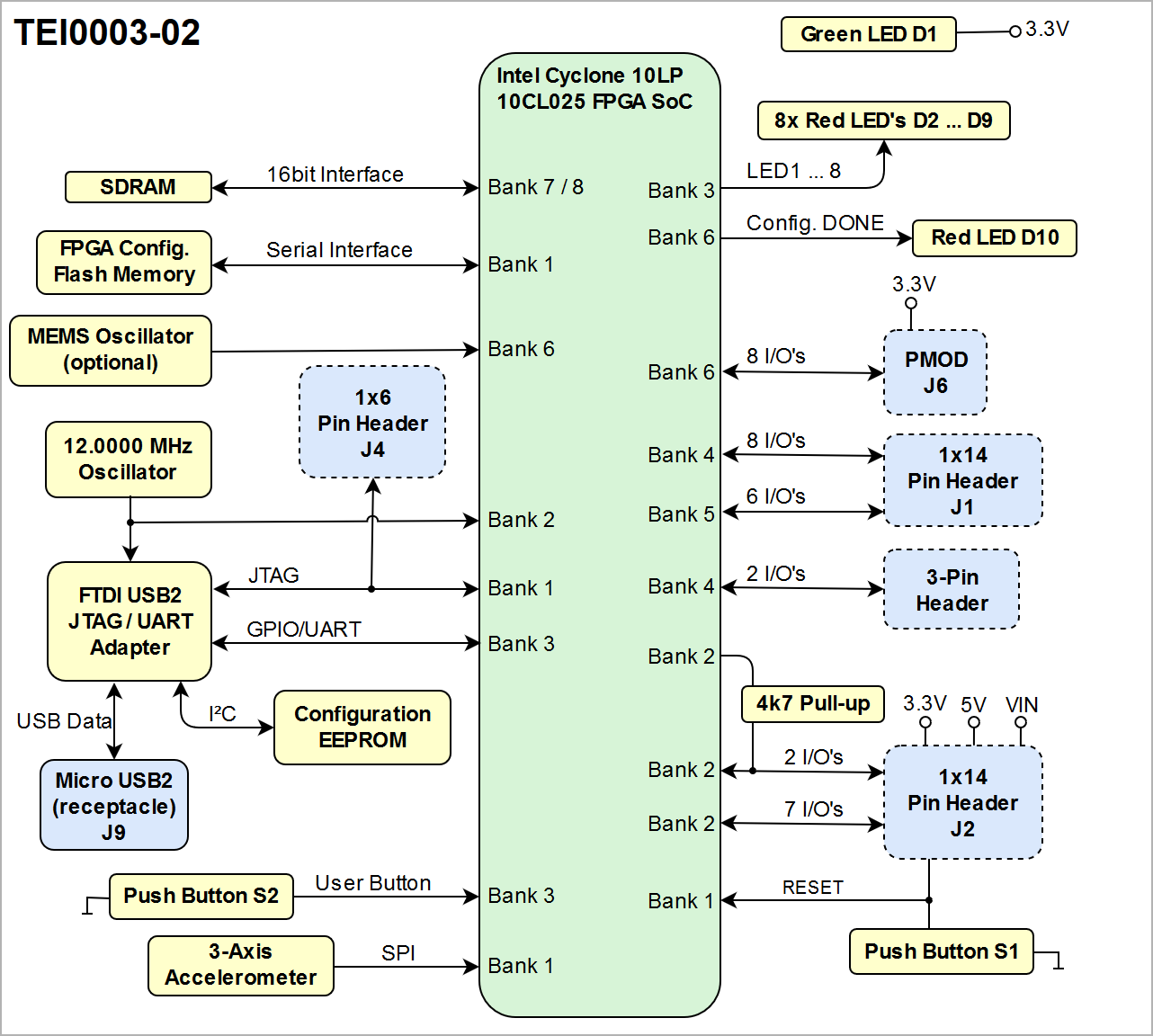 Image Added Image Added
|
|
Main Components
| Scroll Title |
|---|
| anchor | Figure_2 |
|---|
| title | Figure 2: TEI0003-02 FPGA module |
|---|
|
| Scroll Ignore |
|---|
| draw.io Diagram |
|---|
| border | true |
|---|
| viewerToolbar | true |
|---|
| |
|---|
| fitWindow | false |
|---|
| widthdiagramNamelinks | TEI0003 main componentsauto |
|---|
| simpleViewer |
|---|
| tbstyle | hidden |
|---|
| false | | width | lbox | true | |
|---|
| diagramWidth | 641 |
|---|
| revision | 61 |
|---|
|
|
| Scroll Only |
|---|
Image Removed |
|
Main Components
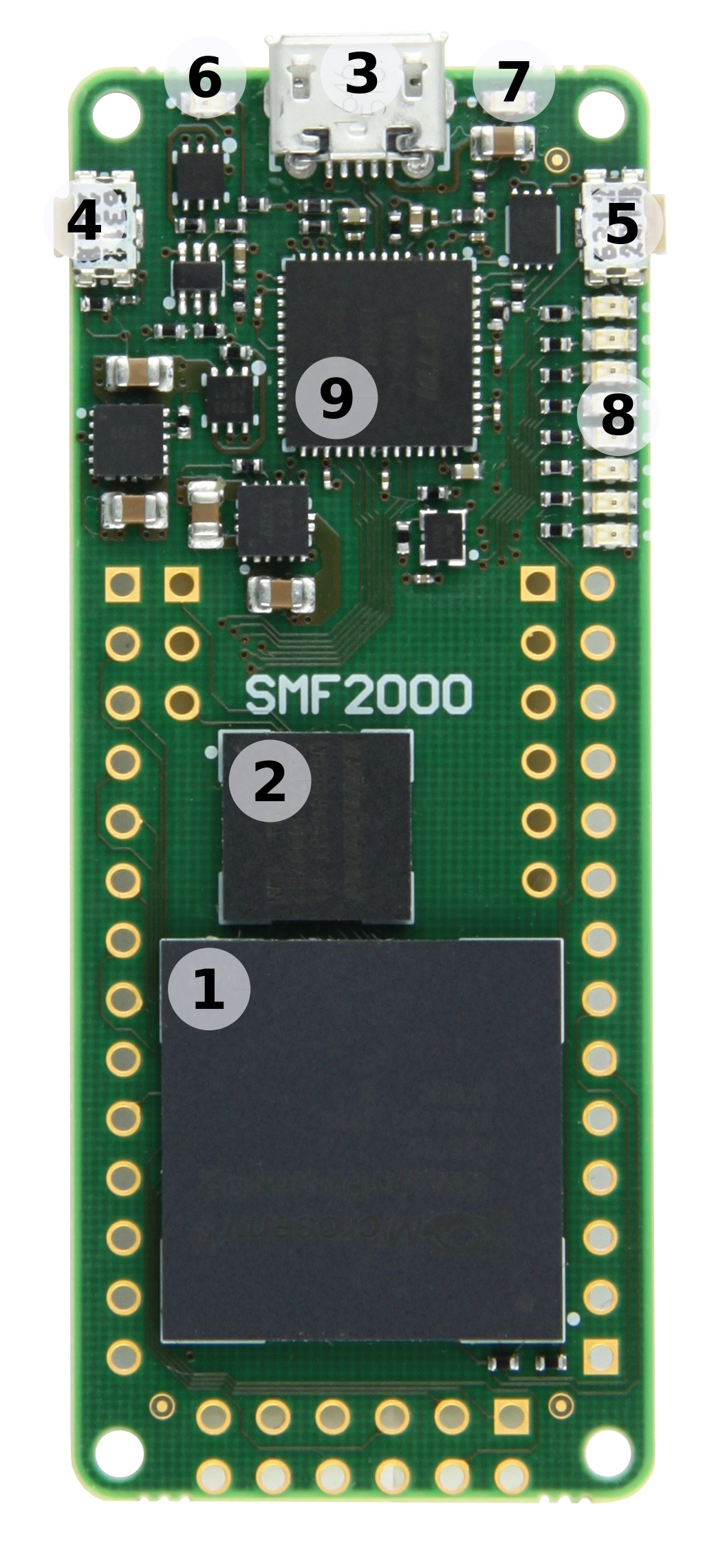 Image Removed
 Image Removed
...
- Microsemi SmartFusion2 FPGA SoC, U5
- 8 Mbyte SDRAM 166MHz, U2
- Micro USB2 B socket (receptacle), J9
- Switch button (reset), S1
- Switch button (user), S2
- Red LED (user), D10
- Green LED (indicating supply voltage), D1
- 8x red LEDs (user), D2 - D9
- FTDI USB2 to JTAG/UART adapter, U3
- 8 Mbyte QSPI Flash memory, U1
- 32.768 KHz auxiliary crystal oscillator, Y1
- 25 MHz main crystal oscillator, Y2
- 1x14 pin header (2.54mm pitch), J2
- 1x6 pin header (2.54mm pitch), J4
- 3-pin header (2.54mm pitch), J3
- 1x14 pin header (2.54mm pitch), J1
- 2x6 Pmod connector, J6
...
| Date | Revision | Contributors | Description |
|---|
| Page info |
|---|
| modified-date |
|---|
| modified-date |
|---|
| dateFormat | yyyy-MM-dd |
|---|
|
| | Page info |
|---|
| infoType | Current version |
|---|
| dateFormat | yyyy-MM-dd |
|---|
| type | Flat |
|---|
|
| | |
...