Page History
...
| HTML |
|---|
<!-- Link to the base folder of the module (remove de/ or en/ from the URL): for example: https://shop.trenz-electronic.de/Download/?path=Trenz_Electronic/Modules_and_Module_Carriers/4x5/4x5_Carriers/TE0703/ --> |
| Scroll Ignore |
|---|
Download PDF version of this document. |
| Scroll pdf ignore | |
|---|---|
Table of Contents
|
...
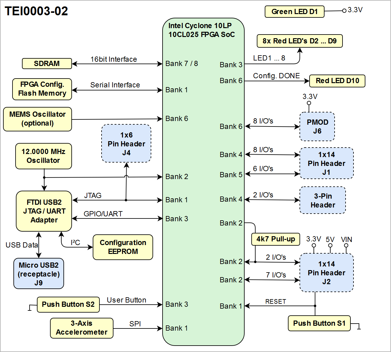
The Trenz Electronic TEI0003 is a low cost small-sized FPGA module integrating a Microsemi SmartFusion2 a Intel Cyclone 10LP 10CL025 FPGA SoC and 8 2 MByte Flash serial memory for configuration and operation.
...
| Scroll Only (inline) |
|---|
Refer to http://trenz.org/cyc1000-info for the current online version of this manual and other available documentation. |
Key Features
Microsemi SmartFusion2 SoC FPGAIntel Cyclone 10LP 10CL025 FPGA SoC
- 8 MByte SDRAM
8 2 MByte QSPI Flash memoryserial configuration memory
- 25 MHz system clock and 32.768 KHz auxiliary clockST Microelectronics LIS3DH MEMS digital output motion sensor
- JTAG and UART over Micro USB2 connector
- 1x 3-1x6 pin header for Live ProbesJTAG access to FPGA SoC
- 1x PMOD header providing 8 GPIOs
2x 14-pin headers (2,54 mm pitch) providing 23 GPIOs
- 1x 3-pin header providing 2 GPIOs
8x 9 user LEDs
- 1 1x user push button
- 3.3V single power supply with on-board voltage regulators
- Size: 61.5 x 25 mm
Additional assembly options are available for cost or performance optimization upon request.
...
| Scroll Title | ||||||||||||||||||||||||||||||
|---|---|---|---|---|---|---|---|---|---|---|---|---|---|---|---|---|---|---|---|---|---|---|---|---|---|---|---|---|---|---|
| ||||||||||||||||||||||||||||||
|
Main Components
| Scroll Title | ||||||||||||||||||||||||||||||
|---|---|---|---|---|---|---|---|---|---|---|---|---|---|---|---|---|---|---|---|---|---|---|---|---|---|---|---|---|---|---|
| ||||||||||||||||||||||||||||||
|
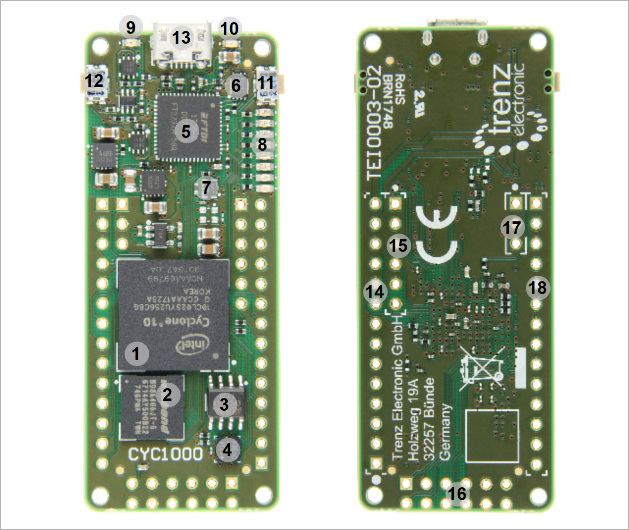
- Intel Cyclone 10LP 10CL025 FPGA SoC, U1
- Winbond W9864G6JT-6
- Microsemi SmartFusion2 FPGA SoC, U5
- 8 Mbyte SDRAM 166MHz, U2
- Micro USB2 B socket (receptacle), J9
- Switch button (reset), S1
- Switch button (user), S2
- Intel EPCQ16ASI8N 2 MByte serial configuration memory, U5
- ST Microelectronics LIS3DH MEMS digital output motion sensor, U4
- FTDI USB2 to JTAG/UART adapter, U3
- Configuration EEPROM for FTDI chip, U9
- 12.0000 MHz oscillator, U7
- 8x red user LEDs, D2 ... D9
- Red LED (Conf. DONERed LED (user), D10
- Green LED (indicating supply voltage), D1
- 8x red LEDs Switch button (user), D2 - D9
- FTDI USB2 to JTAG/UART adapter, U3
- 8 Mbyte QSPI Flash memory, U1
- 32.768 KHz auxiliary crystal oscillator, Y1
- S2
- Switch button (reset), S1
- Micro USB2 B socket (receptacle), J925 MHz main crystal oscillator, Y2
- 1x14 pin header (2.54mm pitch), J2
- 1x6 pin header (2.54mm pitch), J4), J4
- 2x6 Pmod connector, J6
- 3-pin header (2.54mm pitch), J3
- 1x14 pin header (2.54mm pitch), J12x6 Pmod connector, J6
Initial Delivery State
Storage device name | Content | Notes |
|---|---|---|
Quad SPI Flash (U1) OTP areaSerial configuration memory, U5 | DEMO Design | - |
| I2C Configuration EEPROM, U9 | Programmed | - |
...
By default the configuration mode pins of the FPGA are set to QSPI modeload the FPGA design from the serial configuration memory, hence the FPGA is configured from serial Flash configuration memory at system start-up. The JTAG interface of the module is provided for storing the initial FPGA configuration data to the QSPI flash serial configuration memory.
Signals, Interfaces and Pins
...
| Bank | Connector Designator | I/O Signal Count | Bank Voltage | Notes | ||||||
|---|---|---|---|---|---|---|---|---|---|---|
| 1 | J1 | 1 I/O's | 3.3V | - | ||||||
| 21 | J2 | 4 9 I/O's | 3.3V | 2 I/O's of bank | 12 can be pulled-up to 3.3V (4K7 resistors | ) with 2 I/O's of Bank 7 or pins can be shared.|||||
| 2 | J1 | 13 I/O's | 3.3V | - | ||||||
| 2 | J2 | 5 I/O's | 3.3V | - | ||||||
| 2 | J6 | 8 ) with 2 I/O's of same Bank or pins can be shared | ||||||||
| 4 | J1 | 8 | 3.3V | Pmod Connector. | 3 | J4 | 5 I/O's | 3.3V | JTAG interface. | 4- |
| J3 | 2 I/O's | 3.3V | - | |||||||
| 5 | J1 | 6 I/O's | (PROBE A, B) are dedicated to live probes.3.3V | - | ||||||
| 6 | J6 | 8 | 7 | J2 | 2 I/O's | 3.3V | Pmod Connector | |||
| 1 | J4 | 4 | Those 2I/O's | are dedicated to pull-up 23.3V | JTAG interface | |||||
| J2 | 1 I/O's | 3.3V | Reset of bank 1 or pins can be shared. |
Table 2: General overview of single ended I/O signals connected to pin headers and connectors
...
| Bank | VCCIO | I/O's Count | Available on Connectors | Notes |
|---|---|---|---|---|
| 1 | 3.3V | 14 | 5 | 6 I/O's connected to FTDI chip, 1 I/O used for user button S2, 2 I/O's connected to red user LEDs D2 and D10. |
| 2 | 3.3V | 37 | 26 | 6 I/O's user for QSPI Flash, 5 I/O's connected to red user LEDs D3 ... D7. |
| 3 | 3.3V | 5 | 5 | Bank 3 is dedicated to JTAG interface. |
| 4 | 3.3V | 24 | 0 | 2 I/O's are dedicated to live probes, all other I/O's are used as memory interface. |
| 5 | ||||
| 67 | 3.3V | 22 | 2 | 2 I/O's available on header J2, 2 I/O's connected to red user LEDs D8 and D9, all other I/O's are used as memory interface. |
| 7 | ||||
| 8 |
Table 3: General overview of FPGA I/O banks
...
| Clock Source | Schematic Name | Frequency | Clock Input Destination |
|---|---|---|---|
| Microchip MEMS Oscillator, U7 | CLK12M | 12.0000 MHz | FTDI FT2232 U3, pin 3; FPGA SoC bank 2, pin N16 |
ECS SMD Crystal Oscillator, Y1 | - | 32.768 KHz | FPGA SoC U5 auxiliary clock input, pin W17/Y17 |
| AVX Quartz Crystal Oscillator, Y2 | - | 25.000 MHz | FPGA SoC U5 main clock input, pin W18/Y18 |
Table 6: Clock sources overview
...
Overview
Content Tools