Page History
...
The Trenz Electronic TEI0003 is a low cost small-sized FPGA module integrating a Intel Cyclone 10LP 10CL025 FPGA SoC and , 2 MByte serial memory for configuration and operation, 8 MByte SDRAM and a 3-axis accelerometer.
| HTML |
|---|
<!-- Use short link the Wiki Ressource page: for example: http://trenz.org/te0720-info List of available short links: https://wiki.trenz-electronic.de/display/CON/Redirects --> |
...
Intel Cyclone 10LP 10CL025 FPGA SoC
- 8 MByte SDRAM
2 MByte serial configuration memory
- ST Microelectronics LIS3DH MEMS digital output motion sensor3-axis accelerometer
- JTAG and UART over Micro USB2 connector
- 1x6 pin header for JTAG access to FPGA SoC
- 1x PMOD header providing 8 GPIOs
2x 14-pin headers (2,54 mm pitch) providing 23 GPIOs
- 1x 3-pin header providing 2 GPIOs
8x user LEDs
- 1x user push button
- 3.3V single power supply with on-board voltage regulators
- Size: 61.5 x 25 mm
...
- Intel Cyclone 10LP 10CL025 FPGA SoC, U1
- Winbond W9864G6JT 8 Mbyte SDRAM 166MHz, U2
- Intel EPCQ16ASI8N 2 MByte serial configuration memory, U5
- ST Microelectronics LIS3DH MEMS digital output motion sensorLIS3DH 3-axis accelerometer, U4
- FTDI USB2 to JTAG/UART adapter, U3
- Configuration EEPROM for FTDI chip, U9
- 12.0000 MHz oscillator, U7
- 8x red user LEDs, D2 ... D9
- Red LED (Conf. DONE), D10
- Green LED (indicating supply voltage), D1
- Push button (user), S2
- Push button (reset), S1
- Micro USB2 B socket (receptacle), J9
- 1x14 pin header (2.54mm pitch), J2
- 1x6 pin header (2.54mm pitch), J4
- 2x6 Pmod connector, J6
- 3-pin header (2.54mm pitch), J3
- 1x14 pin header (2.54mm pitch), J1
...
On-board serial configuration memory (U5) is provided by Intel EPCQ16ASI8N with 16 MBit (2 MByte) storage capacity. This non volatile memory is used to store initial FPGA configuration via JTAG interface. The memory is connected to FPGA bank 1 via active serial (AS) x1 interface.
SDRAM
The FPGA module is equipped with a Winbond W9864G6JT 64 MBit (8 MByte) SDRAM chip U2. This SDRAM chip is connected to the FPGA bank 7 and 8 via 16-bit memory interface with 166MHz clock frequency and CL3 CAS latency.
FTDI FT2232H IC
The FTDI chip U3 converts signals from USB2.0 to a variety of standard serial and parallel interfaces. Refer to the FTDI data sheet to get information about the capacity of the FT2232H chip.
FTDI FT2232H chip is used in MPPSE mode for JTAG, 2 I/O's of channel A and 6 I/O's of Channel B are routed to FPGA bank 3 of the FPGA SoC and are usable for example as GPIOs, UART or other standard interfaces.
The configuration of FTDI FT2232H chip is pre-programmed on the EEPROM U9.
Motion Sensor
| Serial Memory U5 Pin | Signal Schematic Name | Connected to | Notes |
|---|---|---|---|
| Pin 2, DATA1 | AS_DATA0 | FPGA bank 1, pin H2 | Data out |
| Pin 5, DATA0 | AS_ASDO | FPGA bank 1, pin C1 | Data in |
| Pin 1, nCS | AS_NCS | FPGA bank 1, pin D2 | chip select |
| Pin 6, DCLK | AS_DCLK | FPGA bank 1, pin H1 | clock |
Table 5: Serial configuration memory interface connections
SDRAM
The FPGA module is equipped with a Winbond W9864G6JT 64 MBit (8 MByte) SDRAM chip U2. This SDRAM chip is connected to the FPGA bank 7 and 8 via 16-bit memory interface with 166MHz clock frequency and CL3 CAS latency.
| SDRAM I/O Signals | Signal Schematic Name | Connected to | Notes |
|---|---|---|---|
| Address inputs | A0 ... A13 | bank 8 | - |
| Bank address inputs | BA0 / BA1 | bank 8 | - |
| Data input/output | DQ0 ... DQ15 | bank 7 | - |
| Data mask | DQM0 ... DQM1 | bank 7 | - |
| Clock | CLK | bank 7 | |
| Control Signals | CS | bank 8 | Chip select |
CKE | bank 8 | Clock enable | |
RAS | bank 8 | Row Address Strobe | |
CAS | bank 8 | Column Address Strobe | |
| WE | bank 8 | Write Enable |
Table 6: 16bit SDRAM memory interface
FTDI FT2232H Chip
The FTDI chip U3 converts signals from USB2.0 to a variety of standard serial and parallel interfaces. Refer to the FTDI data sheet to get information about the capacity of the FT2232H chip.
FTDI FT2232H chip is used in MPPSE mode for JTAG, 2 I/O's of channel A and 6 I/O's of Channel B are routed to FPGA bank 3 of the FPGA SoC and are usable for example as GPIOs, UART or other standard interfaces.
The configuration of FTDI FT2232H chip is pre-programmed on the EEPROM U9.
| FTDI Chip U3 Pin | Signal Schematic Name | Connected to | Notes |
|---|---|---|---|
| Pin 12, ADBUS0 | TCK | FPGA bank 1, pin H3 | JTAG interface |
| Pin 13, ADBUS1 | TDI | FPGA bank 1, pin H4 | |
| Pin 14, ADBUS2 | TDO | FPGA bank 1, pin J4 | |
| Pin 15, ADBUS3 | TMS | FPGA bank 1, pin J5 | |
| Pin 17, ADBUS4 | ADBUS4 | FPGA bank 3, pin M8 | user configurable |
| Pin 20, ADBUS7 | ADBUS7 | FPGA bank 3, pin N8 | user configurable |
| Pin 32, BDBUS0 | BDBUS0 | FPGA bank 3, pin | user configurable |
| Pin 33, BDBUS1 | BDBUS1 | FPGA bank 3, pin | user configurable |
| Pin 34, BDBUS2 | BDBUS2 | FPGA bank 3, pin | user configurable |
| Pin 35, BDBUS3 | BDBUS3 | FPGA bank 3, pin | user configurable |
| Pin 37, BDBUS4 | BDBUS4 | FPGA bank 3, pin | user configurable |
| Pin 38, BDBUS5 | BDBUS5 | FPGA bank 3, pin | user configurable |
Table 7: FTDI chip interfaces and pins
3-Axis Accelerometer
On the TEI0003 FPGA board there is a 3-axis accelerometer present. This accelerometer provided by ST Microelectronics LIS3DH and offers many function to detect motion and has also a temperature sensor integrated. It also has a FIFO buffer for storing output data. The sensor is connected to the FPGA through SPI interface and two interrupt lines.
| Accelerometer U4 Pin | Signal Schematic Name | Connected to | Notes |
|---|---|---|---|
| Pin 11, INT1 | SEN_INT1 | FPGA bank 1, pin B1 | Interrupt lines |
| Pin 9, INT2 | SEN_INT2 | FPGA bank 1, pin C2 | |
| Pin 6, SDA/SDI/SDO | SEN_SDI | FPGA bank 1, pin G2 | SPI interface |
| Pin 7, SDO/SA0 | SEN_SDO | FPGA bank 1, pin G1 | |
| Pin 4, SCL/SPC | SEN_SPC | FPGA bank 1, pin F3 | |
| Pin 8, CS | SEN_CS | FPGA bank 1, pin D1 | |
| Pin 13, ADC3 | ADC3 | 5V | Sense 5V input voltage |
Table 8: 3-axis accelerometer interfaces and pinsOn the TEI0003 FPGA board there is a digital output 3-axis motion sensor present. The motion is provided by ST Microelectronics
System Clock Oscillator
The FPGA SoC module has following reference clocking signals provided by on-board oscillators:
| Clock Source | Schematic Name | Frequency | Clock Input Destination |
|---|---|---|---|
| Microchip MEMS Oscillator, U7 | CLK12M | 12.0000 MHz | FTDI FT2232 U3, pin 3; FPGA SoC bank 2, pin M2 |
| optional Microchip MEMS Oscillator, U6 (not fitted) | CLK_X | - | FPGA SoC bank 6, pin E15 |
Table 59: Clock sources overview
On-board LEDs
...
| LED | Color | Signal Schematic Name | FPGA | Notes |
|---|---|---|---|---|
| D1 | Green | - | - | Indicating 3.3V board supply voltage |
| D2 | Red | 'LED1' | bank 6, pin M6 | user |
| D3 | Red | 'LED2' | bank 6, pin T4 | user |
| D4 | Red | 'LED3' | bank 6, pin T3 | user |
| D5 | Red | 'LED4' | bank 6, pin R3 | user |
| D6 | Red | 'LED5' | bank 6, pin T2 | user |
| D7 | Red | 'LED6' | bank 6, pin R4 | user |
| D8 | Red | 'LED7' | bank 6, pin N5 | user |
| D9 | Red | 'LED8' | bank 6, pin N3 | user |
| D10 | Red | 'CONF_DONE' | bank 6, pin H14 | indication configuration is DONE when LED is off |
Table 610: LEDs of the module
Push Buttons
...
| Button | Signal Schematic Name | FPGA | Notes |
|---|---|---|---|
| S1 | 'USER_BTN' | bank 3, pin N6 | user configurable |
| S2 | 'RESET' | bank 1, pin H5 | system reset |
Table 711: Push buttons of the module
...
The FPGA module can be power-supplied through Micro USB2 connector J9 with supply voltage 'USB-VBUS' or alternative through pin header J2 with supply voltage 'VIN'.
The TEM0001 TEI0003 module needs one single power supply of 5.0V nominal.
...
Board size: PCB 25mm × 61,5mm. Notice that some parts the are hanging slightly over the edge of the PCB like the the Micro USB2 B connector, which determine the total physical dimensions of the carrier board. Please download the assembly diagram for exact numbers.
PCB thickness: ca. 1.65mm
Highest part on the PCB without fitted headers and connectors is the Micro USB2 B connector, which has an approximately hight of 3 mm. Please download the step model for exact numbers.
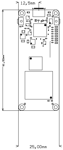
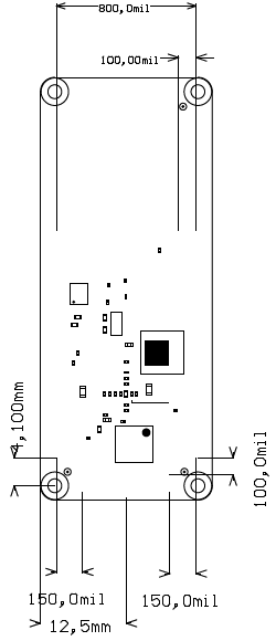
Figure 4: Module physical dimensions drawing
...
Overview
Content Tools