Page History
...
On-board serial configuration memory (U5) is provided by Intel EPCQ16ASI8N with 16 MBit (2 MByte) storage capacity. This non volatile memory is used to store initial FPGA configuration via JTAG interface. The memory is connected to FPGA bank 1 via active serial (AS) x1 interface.
| Serial Memory U5 Pin | Signal Schematic Name | Connected to | Notes |
|---|---|---|---|
| Pin 2, DATA1 | AS_DATA0 | FPGA bank 1, pin H2 | Data out |
| Pin 5, DATA0 | AS_ASDO | FPGA bank 1, pin C1 | Data in |
| Pin 1, nCS | AS_NCS | FPGA bank 1, pin D2 | chip select |
| Pin 6, DCLK | AS_DCLK | FPGA bank 1, pin H1 | clock |
Table 5: Serial configuration memory interface connections
...
The FPGA module is equipped with a Winbond W9864G6JT 64 MBit (8 MByte) SDRAM chip U2. This SDRAM chip is connected to the FPGA bank 7 and 8 via 16-bit memory interface with 166MHz clock frequency and CL3 CAS latency.
| SDRAM I/O Signals | Signal Schematic Name | Connected to | Notes |
|---|---|---|---|
| Address inputs | A0 ... A13 | bank 8 | - |
| Bank address inputs | BA0 / BA1 | bank 8 | - |
| Data input/output | DQ0 ... DQ15 | bank 7 | - |
| Data mask | DQM0 ... DQM1 | bank 7 | - |
| Clock | CLK | bank 7 | |
| Control Signals | CS | bank 8 | Chip select |
CKE | bank 8 | Clock enable | |
RAS | bank 8 | Row Address Strobe | |
CAS | bank 8 | Column Address Strobe | |
| WE | bank 8 | Write Enable |
Table 6: 16bit SDRAM memory interface
...
The configuration of FTDI FT2232H chip is pre-programmed on the EEPROM U9.
| FTDI Chip U3 Pin | Signal Schematic Name | Connected to | Notes |
|---|---|---|---|
| Pin 12, ADBUS0 | TCK | FPGA bank 1, pin H3 | JTAG interface |
| Pin 13, ADBUS1 | TDI | FPGA bank 1, pin H4 | |
| Pin 14, ADBUS2 | TDO | FPGA bank 1, pin J4 | |
| Pin 15, ADBUS3 | TMS | FPGA bank 1, pin J5 | |
| Pin 17, ADBUS4 | ADBUS4 | FPGA bank 3, pin M8 | user configurable |
| Pin 20, ADBUS7 | ADBUS7 | FPGA bank 3, pin N8 | user configurable |
| Pin 32, BDBUS0 | BDBUS0 | FPGA bank 3, pin | user configurable |
| Pin 33, BDBUS1 | BDBUS1 | FPGA bank 3, pin | user configurable |
| Pin 34, BDBUS2 | BDBUS2 | FPGA bank 3, pin | user configurable |
| Pin 35, BDBUS3 | BDBUS3 | FPGA bank 3, pin | user configurable |
| Pin 37, BDBUS4 | BDBUS4 | FPGA bank 3, pin | user configurable |
| Pin 38, BDBUS5 | BDBUS5 | FPGA bank 3, pin | user configurable |
Table 7: FTDI chip interfaces and pins
...
On the TEI0003 FPGA board there is a 3-axis accelerometer present. This accelerometer provided by ST Microelectronics LIS3DH and offers many function to detect motion and has also a temperature sensor integrated. It also has a FIFO buffer for storing output data. The sensor is connected to the FPGA through SPI interface and two interrupt lines.
| Accelerometer U4 Pin | Signal Schematic Name | Connected to | Notes |
|---|---|---|---|
| Pin 11, INT1 | SEN_INT1 | FPGA bank 1, pin B1 | Interrupt lines |
| Pin 9, INT2 | SEN_INT2 | FPGA bank 1, pin C2 | |
| Pin 6, SDA/SDI/SDO | SEN_SDI | FPGA bank 1, pin G2 | SPI interface |
| Pin 7, SDO/SA0 | SEN_SDO | FPGA bank 1, pin G1 | |
| Pin 4, SCL/SPC | SEN_SPC | FPGA bank 1, pin F3 | |
| Pin 8, CS | SEN_CS | FPGA bank 1, pin D1 | |
| Pin 13, ADC3 | ADC3 | 5V | Sense 5V input voltage |
Table 8: 3-axis accelerometer interfaces and pins
...
There are following dependencies how the initial voltage of the extern power supply is distributed to the on-board DCDC converters: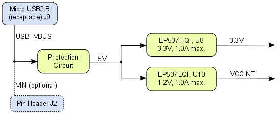
| Scroll Title | ||||||||||||||||||||||||
|---|---|---|---|---|---|---|---|---|---|---|---|---|---|---|---|---|---|---|---|---|---|---|---|---|
| ||||||||||||||||||||||||
|
Figure 3: Power Distribution Diagram
...
Overview
Content Tools