Page History
...
Intel Cyclone 10LP 10CL025 FPGA SoC
- 8 MByte SDRAM
2 MByte serial configuration memory
- ST Microelectronics LIS3DH 3-axis accelerometer
- JTAG and UART over Micro USB2 connector
- 1x6 pin header for JTAG access to FPGA SoC
- 1x PMOD header providing 8 GPIOs
2x 14-pin headers (2,54 mm pitch) providing 23 GPIOs
- 1x 3-pin header providing 2 GPIOs
8x user LEDs
- 1x user push button
- 35.3V 0V single power supply with on-board voltage regulators
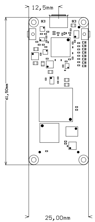
- Size: 61.5 x 25 mm
...
| Scroll Title | ||||||||||||||||||||||||||||||
|---|---|---|---|---|---|---|---|---|---|---|---|---|---|---|---|---|---|---|---|---|---|---|---|---|---|---|---|---|---|---|
| ||||||||||||||||||||||||||||||
|
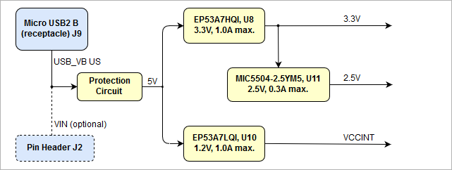
Power Consumption
...
There is no specific or special power-on sequence, just one single power source is needed.
Power Rails
| Connector Designator | VCC / VCCIO Schematic Name | Voltage | Direction | Pins | Notes |
|---|---|---|---|---|---|
| J2 | 5V | 5.0V | Out | Pin 14 | - |
| VIN | 5.0V | In | Pin 13 | - | |
| 3.3V | 3.3V | Out | Pin 12 | - | |
| J6 | 3.3V | 3.3V | Out | Pin 6, 12 | - |
| J9 | USB_VBUS | 5.0V | In | Pin 1 | - |
Table 13: Connector power pin description
Bank Voltages
Bank | Voltage | Voltage Range |
|---|---|---|
| 1 | 3.3V | all bank voltages fixed |
| 2 | 3.3V | |
| 3 | 3.3V | |
| 4 | 3.3V | |
| 5 | 3.3V | |
| 6 | 3.3V | |
| 7 | 3.3V | |
| 8 | 3.3V |
Table 14: FPGA SoC VCCO bank voltages
...
Parameter | Min | Max | Units | Reference document |
|---|---|---|---|---|
VIN supply voltage (5.0V nominal) | -0.3 | 6.0 | V | EP53A7HQI / EP53A7LQI datasheet |
| I/O Input voltage for FPGA I/O bank | -0.35 | 34.632 | V | Intel Cyclone 10 LP datasheet |
Storage Temperature | -40 | +90 | °C | LED R6C-AL1M2VY/3T datasheet |
Table 1315: Absolute maximum ratings
...
| Parameter | Min | Max | Units | Reference document |
|---|---|---|---|---|
| VIN supply voltage (5.0V nominal) | 4.75 | 5.25 | V | same as USB-VBUS specification |
| I/O Input voltage for FPGA I/O bank | 0–0.5 | 3.456 | V | Intel Cyclone 10 LP datasheet |
| Operating temperature range | 0 | +70 | °C | Winbond datasheet W9864G6GT |
Table 1416: Recommended operating conditions
| Note |
|---|
| Please check Intel Cyclone 10 LP datasheet for complete list of absolute maximum and recommended operating ratings for the FPGA device. |
...
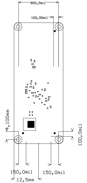
Board size: PCB 25mm × 61,5mm. Notice that some parts the are hanging slightly over the edge of the PCB like the the Micro USB2 B connector, which determine the total physical dimensions of the carrier board. Please download the assembly diagram for exact numbers.
PCB thickness: ca. 1.65mm
Highest part on the PCB without fitted headers and connectors is the Micro USB2 B connector, which has an approximately hight of 3 mm. Please download the step model for exact numbers.
| Scroll Title | ||||
|---|---|---|---|---|
| ||||
|
Revision History
Hardware Revision History
| Date | Revision | Notes | PCN | Documentation Link |
|---|---|---|---|---|
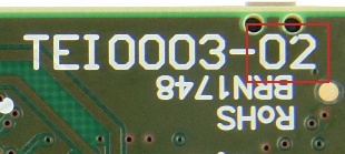
| - | 02 | Second First Production Release | - | TEI0003-02 |
| - | 01 | First Production ReleasePrototypes | - | TEI0003-01 |
Table 1217: Module hardware revision history
Hardware revision number is printed on the PCB board together with the module model number separated by the dash.
| Scroll Title | ||||
|---|---|---|---|---|
| ||||
|
Document Change History
| Date | Revision | Contributors | Description | ||||||||||||||||
|---|---|---|---|---|---|---|---|---|---|---|---|---|---|---|---|---|---|---|---|
|
| Ali Naseri |
|
Table 1318: Document change history
Disclaimer
...
Overview
Content Tools