Page History
...
Intel Cyclone 10LP 10CL025 FPGA SoC
- 8 MByte SDRAM
2 8 MByte serial configuration QSPI Flash memory
- ST Microelectronics LIS3DH 3-axis accelerometer
- JTAG and UART over Micro USB2 connector
- 1x6 pin header for JTAG access to FPGA SoC
- 1x PMOD header providing 8 GPIOs
2x 14-pin headers (2,54 mm pitch) providing 23 GPIOs22 GPIOs with 7 analog inputs as alternative function
- 1x 3-pin header providing 2 GPIOsanalog inputs or 1 GPIO
8x user LEDs
- 1x user push button
- 5.0V single power supply with on-board voltage regulators
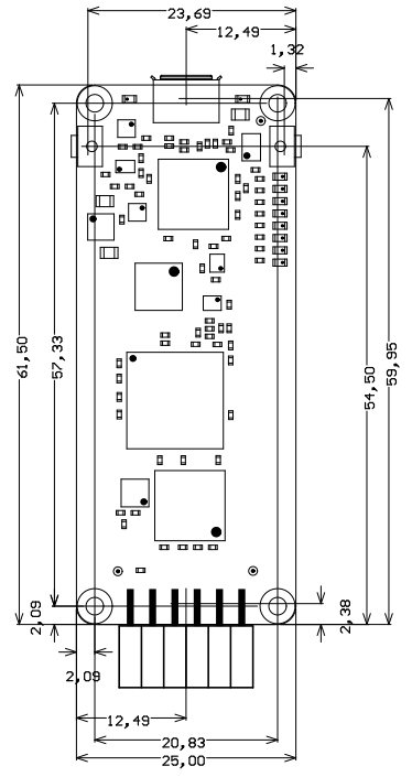
- Size: 61.5 x 25 mm
...
| Scroll Title | ||||||||||||||||||||||||||||||
|---|---|---|---|---|---|---|---|---|---|---|---|---|---|---|---|---|---|---|---|---|---|---|---|---|---|---|---|---|---|---|
| ||||||||||||||||||||||||||||||
|
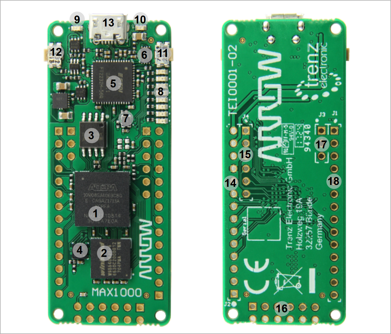
- Intel Cyclone 10LP 10CL025 MAX10 10M08 FPGA SoC, U1
- Winbond W9864G6JT 8 Mbyte SDRAM 166MHz, U2
- Intel EPCQ16ASI8N 2 MByte serial configuration 8 Mbyte QSPI Flash memory, U5
- ST Microelectronics LIS3DH 3-axis accelerometer, U4
- FTDI USB2 to JTAG/UART adapter, U3
- Configuration EEPROM for FTDI chip, U9
- 12.0000 MHz oscillator, U7
- 8x red user LEDs, D2 ... D9
- Red LED (Conf. DONE), D10
- Green LED (indicating supply voltage), D1
- Push button (user), S2
- Push button (reset), S1
- Micro USB2 B socket (receptacle), J9
- 1x14 pin header (2.54mm pitch), J2
- 1x6 pin header (2.54mm pitch), J4
- 2x6 Pmod connector, J6
- 3-pin header (2.54mm pitch), J3
- 1x14 pin header (2.54mm pitch), J1
...
Storage device name | Content | Notes |
|---|---|---|
Serial configuration memoryQuad SPI Flash, U5 | DEMO Design | - |
| I2C Configuration EEPROM, U9 | Programmed | - |
...
| Scroll Title | ||||||||||||||||||||||||
|---|---|---|---|---|---|---|---|---|---|---|---|---|---|---|---|---|---|---|---|---|---|---|---|---|
| ||||||||||||||||||||||||
|
Power Consumption
| FPGA | Design | Typical Power, 25C ambient |
|---|---|---|
| Intel Cyclone 10LP 10CL025 FPGA SoC | Not configured | TBD* |
...
Table 16: Recommended operating conditions
| Note |
|---|
| Please check Intel Cyclone 10 LP MAX10 datasheet for complete list of absolute maximum and recommended operating ratings for the FPGA device. |
Physical Dimensions
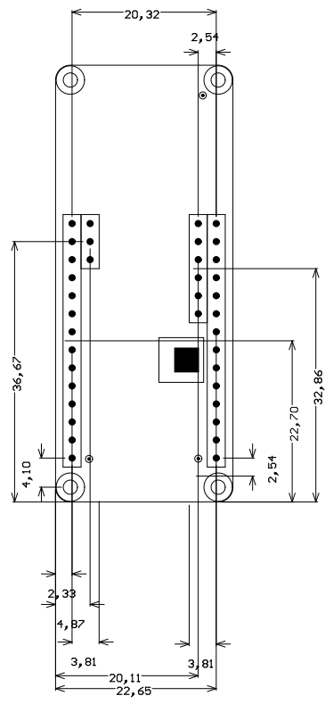
Please note that two different units are used on the figures below, SI system millimeters (mm) and imperial system thousandths of an inch(mil). This is because of the 100mil pin headers used, see also explanation below. To convert mils to millimeters and vice versa use formula 100mil's = 2,54mm.
Board size: PCB 25mm × 61,5mm. Notice that some parts the are hanging slightly over the edge of the PCB like the the Micro USB2 B connector, which determine the total physical dimensions of the carrier board. Please download the assembly diagram for exact numbers.
PCB thickness: ca. 1.65mm
Highest part on the PCB without fitted headers and connectors is the Micro USB2 B connector, which has an approximately hight of 3 mm. Please download the step model for exact numbers.
...
| Scroll Title | ||||
|---|---|---|---|---|
| ||||
|
Revision History
Hardware Revision History
| Date | Revision | Notes | PCN | Documentation Link |
|---|---|---|---|---|
| - | 03 | Current available revision | - | TEI0001-03 |
| - | 02 | First Production Release | - | TEI0003TEI0001-02 |
| - | 01 | Prototypes | - | TEI0001-01 |
Table 17: Module hardware revision history
...
Overview
Content Tools