Versions Compared
Key
- This line was added.
- This line was removed.
- Formatting was changed.
HTML |
---|
<!--
Template Revision 1.6
--> |
Scroll Only (inline) |
---|
Online version of this manual and other related documents can be found at https://wiki.trenz-electronic.de/display/PD/SC-CPLD-Firmware |
Scroll pdf ignore | ||||
---|---|---|---|---|
Table of contents
|
Custom_table_size_100 |
---|
Page properties | ||||
---|---|---|---|---|
| ||||
Template Revision 2.1 Design Name always "TE Series Name" + optional CPLD Name + "CPLD"
|
Overview
CPLD Device with designator U21: LCMX02-256HC
Feature Summary
- JTAG routing
- Boot Mode settings
- LED
Firmware Revision and supported PCB Revision
See Document Change History
Product Specification
Port Description
Name / opt. VHD Name | Direction | Pin | Pullup/Down | Bank Power | Description | Note: PCB REV04 REV05 Connection | Note: PCB REV01 REV02 Connection |
---|---|---|---|---|---|---|---|
C_TCK | in | 30 | DOWN | 3.3VIN | JTAG B2B | ||
C_TDI | in | 32 | DOWN | 3.3VIN | JTAG B2B | ||
C_TDO | out | 1 | DOWN | 3.3VIN | JTAG B2B | ||
C_TMS | in | 29 | DOWN | 3.3VIN | JTAG B2B |
...
RST_EN | inout |
...
27 | NONE | 3.3VIN | Reset pin output to reset FPGA via CPLD chip | For PCB REV04 EN1(input) (pulled up in CPLD) / For PCB REV05 REST_EN(output) (Floating in CPLD) Power Enable from B2B Connector (Positive Enable |
...
) (input pin) for PCB revision 04 in this case used only for PGOOD feedback / Reset pin (output pin) for PCB revision 5 in this case this pin is reset pin that is activated by firmware and not by hardware after changing the boot mode via software. | |||||||
User_LED | out | 4 | NONE | 3.3VIN | user defined or status, see LED description | For PCB REV04 shows the state of X1 and X0. / For PCB REV05 shows the boot mode state for selection via hardware (Dip switch in carrier board) or via software (related command in linux console or FSBL code) | 1.8V input ERR_OUT(PS_ERROR_OUT) |
...
PG_ALL | in | 5 | NONE | 3.3VIN | This pin is used as power good (input) |
...
Unused in CPLD firmware for PCB REV04( In hardware is pulled up) / Used in PCB REV05 as power good input pin | 1.8V input ERR_STATUS as input | ||||||
JTAGEN | in | 26 | --- | 3.3VIN | Enable JTAG access to CPLD for Firmware update (zero: JTAG routed to module, one: CPLD access) | ||
MODE | in | 25 | UP | 3.3VIN | Boot Mode for Zynq/ZynqMP Devices (Flash or SD) | ||
MODE0 | out | 12 | DOWN | 1.8V | ZynqMP Boot Mode Pin 0 | ||
MODE1 | out | 13 | DOWN | 1.8V | ZynqMP Boot Mode Pin 1 | ||
MODE2 | out | 14 | DOWN | 1.8V | ZynqMP Boot Mode Pin 2 | ||
MODE3 | out | 16 | DOWN | 1.8V | ZynqMP Boot Mode Pin 3 | ||
NOSEQ | inout | 23 | UP | 3.3VIN |
...
Usage CPLD Variant depends |
...
Used as GPIO pin by user. This pin can be written or read via i2cset command in linux console or FSBl code functions. | Used as boot mode selection pin, if CPLD is programmed using SC0820_qspi_sd_jtag.jed jed-file. | ||||
PGOOD | inout | 28 | UP | 3.3VIN | Module Power Good (only Feedback from EN1 for PCB revision 4 or older). / For PCB revision 5 is used as boot mode selection pin or power good pin (feedback from PG_ALL pin) |
...
Module Power Good (only Feedback from EN1 for PCB revision 4 or older). / Boot mode selection pin for PCB REV05 | |||||||
PHY_LED1 | in | 17 | --- | 1.8V | ETH PHY LED1 / currently_not_used | ||
TCK | out | 9 | DOWN | 1.8V | JTAG ZynqMP | ||
TDI | out | 8 | DOWN | 1.8V | JTAG ZynqMP | ||
TDO | in | 10 | DOWN | 1.8V | JTAG ZynqMP | ||
TMS | out | 11 | DOWN | 1.8V | JTAG ZynqMP | ||
X0 | in | 20 | UP | VCCO_65 |
...
I2C SCL pin | Used as tri-state enable-input for User_LED pin for PCB REV04 / Used as i2c SCL pin for PCB REV05 | ||
X1 | inout | 21 | UP |
...
VCCO_65 |
...
I2C SDA pin | Used as tri-state input for User_LED pin for PCB REV04 / Used as i2c SDA pin for PCB REV05 |
Functional Description
JTAG
JTAG signals routed directly through the CPLD to FPGA. Access between CPLD and FPGA can be multiplexed via JTAGEN (logical one for CPLD, logical zero for FPGA) on JM1-89.
Boot Mode
Boot
...
mode can be set either by hardware (dip-switch) on the carrier board or by firmware in linux console or FSBL code. Even after booting boot mode can be changed . After changing the boot mode FPGA is restarted automatically by CPLD, if PCB revision is REV05, otherwise for PCB revision 4 user must reset manually to execute boot mode changing correctly.To change boot mode a state machine continuously monitors the corresponding register that can be change via I2C interface between CPLD and FPGA.
Change method | Boot Mode | CPLD PGOOD Pin (B2B Pin JM1-30) | CPLD MODE Pin (B2B Pin JM1-32) | Description |
---|---|---|---|---|
Hardware | JTAG | 0 | 0 | |
Hardware | eMMC | 0 | 1 | |
Hardware | SD Card | 1 | 0 | |
Hardware | QSPI | 1 | 1 |
Change method | Boot Mode | Command in linux console | Command in FSBL | Description |
---|---|---|---|---|
Software | JTAG | i2cset -y 1 0x20 0x01 0x91 | iic_write8(0x20,0x01,0x91) | 0x20 is device address. 0x01 is register address. |
Software | SD Card | i2cset -y 1 0x20 0x01 0x93 | iic_write8(0x20,0x01,0x93) | 0x20 is device address. 0x01 is register address. |
Software | QSPI | i2cset -y 1 0x20 0x01 0x92 | iic_write8(0x20,0x01,0x92) | 0x20 is device address. 0x01 is register address. |
Software | eMMC | i2cset -y 1 0x20 0x01 0x90 | iic_write8(0x20,0x01,0x90) | 0x20 is device address. 0x01 is register address. |
If PCB revision is REV04, then user must reset manually the carrier board after changing the boot mode using i2cset command in linux console. If PCB revision is REV05, it is not necessary to reset the FPGA by user, because FPGA will be reset automatically via CPLD after changing the boot mode via i2cset command in linux console.
...
SD/QSPI
(default Firmware)
...
For other UltraScale+ Boot Modes options custom firmware is needed, see also Table 11.1 Boot Modes from Xilinx UG1085.
Note |
---|
A special FSBL is provided on 2017.4 or newer reference designs to write boot image to QSPI with Xilinx tools (Vivado or SDK) on Boot Mode unequal JTAG . |
Note |
---|
NOSEQ*: Please check the carrier board documentation, before using the SD/QSPI/JTAG firmware variant on TE0820. In the most cases special carrier CPLD firmware is needed. |
Power
...
Power
For PCB revision 4 or older PGOOD depends on EN1. There is no additional power management controlled by CPLD. For PCB revision 5 PGOOD depends on PG_ALL signal.
LED
LED glows depending on boot mode and whether boot mode is selected by hardware or firmware.
LED state | Condition |
---|
...
*It's recommended to forward this signal to a carrier LED if status check is needed.
...
Related command | Description | ||
---|---|---|---|
OFF | JTAG boot mode and software boot mode selection not active | Boot mode is adjusted by dip switch on the carrier board. | CPLD_BM = '0' |
Blink sequence *ooooooo | QSPI boot mode and software boot mode selection not active | Boot mode is adjusted by dip switch on the carrier board. | CPLD_BM = '0' |
Blink sequence **oooooo | eMMC boot mode and software boot mode selection not active | Boot mode is adjusted by dip switch on the carrier board. | CPLD_BM = '0' |
Blink sequence ***ooooo | SD card boot mode and software boot mode selection not active | Boot mode is adjusted by dip switch on the carrier board. | CPLD_BM = '0' |
Blink sequence ****oooo | JTAG boot mode and software boot mode selection active | i2cset -y 1 0x20 0x01 0x91 in linux console | CPLD_BM = '1' |
Blink sequence *****ooo | QSPI boot mode and software boot mode selection active | i2cset -y 1 0x20 0x01 0x92 in linux console | CPLD_BM = '1' |
Blink sequence ******** | eMMC boot mode and software boot mode selection active | i2cset -y 1 0x20 0x01 0x93 in linux console | CPLD_BM = '1' |
ON | SD card boot mode and software boot mode selection active | i2cset -y 1 0x20 0x01 0x90 in linux console | CPLD_BM = '1' |
I2C interface
CPLD firmware consists of a i2c t GPIO block. This subsystem provides i2c protocol interface to 32-bit (4 x 8-bit) (GPIO_input[31:0]) registers for reading from CPLD and (4 x 8-bit) (GPIO_output[31:0]) registers for writing in CPLD as general purpose parallel input and output (I/Os). The written and read data is communicated from/to FPGA via i2c bus interface protocol. The address of this block in the firmware is 0x20.In this case related i2c bus is bus 1.
draw.io Diagram | ||||||||||||||||||||
---|---|---|---|---|---|---|---|---|---|---|---|---|---|---|---|---|---|---|---|---|
|
Register | Direction in CPLD | Address |
---|---|---|
GPIO_input[7:0] | Output (reading from CPLD) | 0x00 |
GPIO_input[15:8] | Output (reading from CPLD) | 0x01 |
GPIO_input[23:16] | Output (reading from CPLD) | 0x02 |
GPIO_input[31:24] | Output (reading from CPLD) | 0x03 |
GPIO_output[7:0] | Input (writing to CPLD) | 0x00 |
GPIO_output[15:8] | Input (writing to CPLD) | 0x01 |
GPIO_output[23:16] | Input (writing to CPLD) | 0x02 |
GPIO_output[31:24] | Input (writing to CPLD) | 0x03 |
NOSEQ pin
This pin in PCB REV04 with old CPLD firmware version (REV04) is used as boot mode pin select. If CPLD is programmed with SC0820_qspi_sd_jtag.jed as jed file and NOSEQ is high, JTAG boot mode will be selected. For PCB REV05 or PCB REV04 with new CPLD firmware (CPLD firmware REV05) NOSEQ pin can be used by user as GPIO pin and accessed via i2c interface. In this case the following table can be used:
NOSEQ pin as output | Condition | Command in linux console |
---|---|---|
'1' | GPIO_output(16) = '1' | i2cset -y 1 0x20 0x02 0x01 |
'0' | GPIO_output(16) = '0' | i2cset -y 1 0x20 0x02 0x00 |
NOSEQ pin as input | Description | Command in linux console |
Reading state of NOSEQ pin | GPIO_input(16) = NOSEQ | i2cget -y 1 0x20 0x02 |
Access to CPLD Registers
CPLD registers can be accessed via i2c interface. In the following table is shown how these registers can be read or written:
Register | Direction in CPLD | Address | Related instruction in linux console to access the register |
---|---|---|---|
GPIO_input[7:0] | Output (reading from CPLD) | 0x00 | i2cget -y 1 0x20 0x00 |
GPIO_input[15:8] | Output (reading from CPLD) | 0x01 | i2cget -y 1 0x20 0x01 |
GPIO_input[23:16] | Output (reading from CPLD) | 0x02 | i2cget -y 1 0x20 0x02 |
GPIO_input[31:24] | Output (reading from CPLD) | 0x03 | i2cget -y 1 0x20 0x03 |
GPIO_output[7:0] | Input (writing to CPLD) | 0x00 | i2cset -y 1 0x20 0x00 <data> |
GPIO_output[15:8] | Input (writing to CPLD) | 0x01 | i2cset -y 1 0x20 0x01 <data> |
GPIO_output[23:16] | Input (writing to CPLD) | 0x02 | i2cset -y 1 0x20 0x02 <data> |
GPIO_output[31:24] | Input (writing to CPLD) | 0x03 | i2cset -y 1 0x20 0x03 <data> |
Some of these registers are using to show some information same as CPLD revision and boot mode while booting.
Register | Address | related data | Read/write by user | Description |
---|---|---|---|---|
GPIO_input[7:0] | 0x00 | CPLD REVISION (8 bits) | No | |
GPIO_input[15:8] | 0x01 | "00" & BOOTMODE_GEN (2 bits) & PUDC (1 bit) & CPLD_BM (1 bit) & BOOT_MODE (2 bits) | No | BOOTMODE_GEN is a generic parameter in firmware code to select type of jed-file. For example if this parameter is 3 , then by programming the related jed-file the user can have all boot mode options. (QSPI/JTAG/SD Card/eMMC). PUDC is the state of PUDC pin of FPGA. CPLD_BM is a parameter to show if boot mode selection is executed via hardware ( if low) or software (if high) BOOT_MODE shows selected boot mode. |
GPIO_input8[16] | 0x02 | NOSEQ pin | Yes | |
Register | Address | related data | Description | |
GPIO_output[16] | 0x02 | NOSEQ pin | Yes |
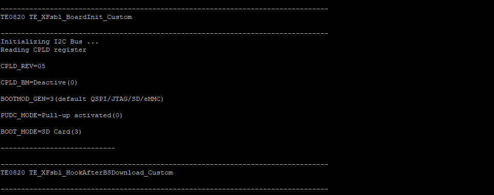
If CPLD firmware version is REV05, then boot mode, CPLD revision and some features of the board will be displayed in the linux console via FSBL code while booting. The format of these informations are shown in the following:
Information | Displayed in Linux console | Description |
---|---|---|
CPLD Revision | CPLD_REV = <cpld revision> | |
Boot mode selection procedure | CPLD_BM = < bm selection procedure> |
|
Jed file that on CPLD is programmed | BOOTMODE_GEN = < jed file type> |
|
PUDC pin state | PUDC_MODE = <pudc state> |
|
Boot mode | BOOT_MODE = <boot mode> |
|
The CPLD revision, boot mode and other informations will be displayed while booting as shown:
Scroll Title | ||||
---|---|---|---|---|
| ||||
Image Added |
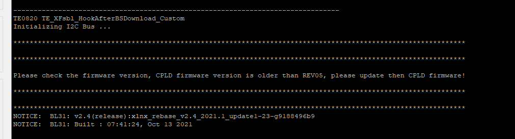
If PCB revision is REV04 and CPLD firmware version is older than REV05 (for example REV04) , then it will not be displayed these informations same as boot mode while booting and the following message will be displayed:
Scroll Title | ||||
---|---|---|---|---|
| ||||
Image Added |
...
Appx. A: Change History
For PCB REV01 and REV02 Documentation available on: TE0820-REV01_REV02 CPLD
Revision Changes
- REV04 to REV05
Adding configuration of boot mode in linux console and via generic parameters
PGOOD pin used as boot mode selector pin.
Adding boot mode configuration via hardware
JTAG time constraint correction
Adding i2c to gpio ip (i2c_slave.vhd)
LED function is changed.
New generic parameter defined : PCB_REV
EN1 pin
is renamed to RST_EN.
pin is input for PCB_REV=4 and it is enable pin same as before.
is reset output for PCB_REV=5 or newer.
- REV03 to REV04
- PCB REV03 support only
X1 is input for USER LED
X0 select X0 or Firmware Blink status to User LE
blink modes for QSPI/SD firmware
- REV02 to REV03
- new Boot Mode variants
- new X0 status blink sequencing
- REV01 to REV02
- Boot Mode variants
- X1
- Remove ERR_STATUS
Document Change History
To get content of older revision got to "Change History" of this page and select older document revision number.
Page properties | ||||
---|---|---|---|---|
| ||||
|
Date | Document Revision | CPLD Firmware Revision | Supported PCB Revision | Authors | Description | ||||||||||||||
---|---|---|---|---|---|---|---|---|---|---|---|---|---|---|---|---|---|---|---|
|
| REV05 | REV04 |
...
,REV05 |
|
| |||||||||
2018-08-29 | v.2 | REV04 | REV03 | John Hartfiel |
| ||||||
v.1 | REV04 | REV03 | John Hartfiel |
| |||||||
v.1 | REV04 | REV03 |
|
| |||||||
All |
|
Appx. B: Legal Notices
Include Page | ||||
---|---|---|---|---|
|
Scroll Only | ||
---|---|---|
|
Scroll pdf ignore | ||||||
---|---|---|---|---|---|---|
|