...
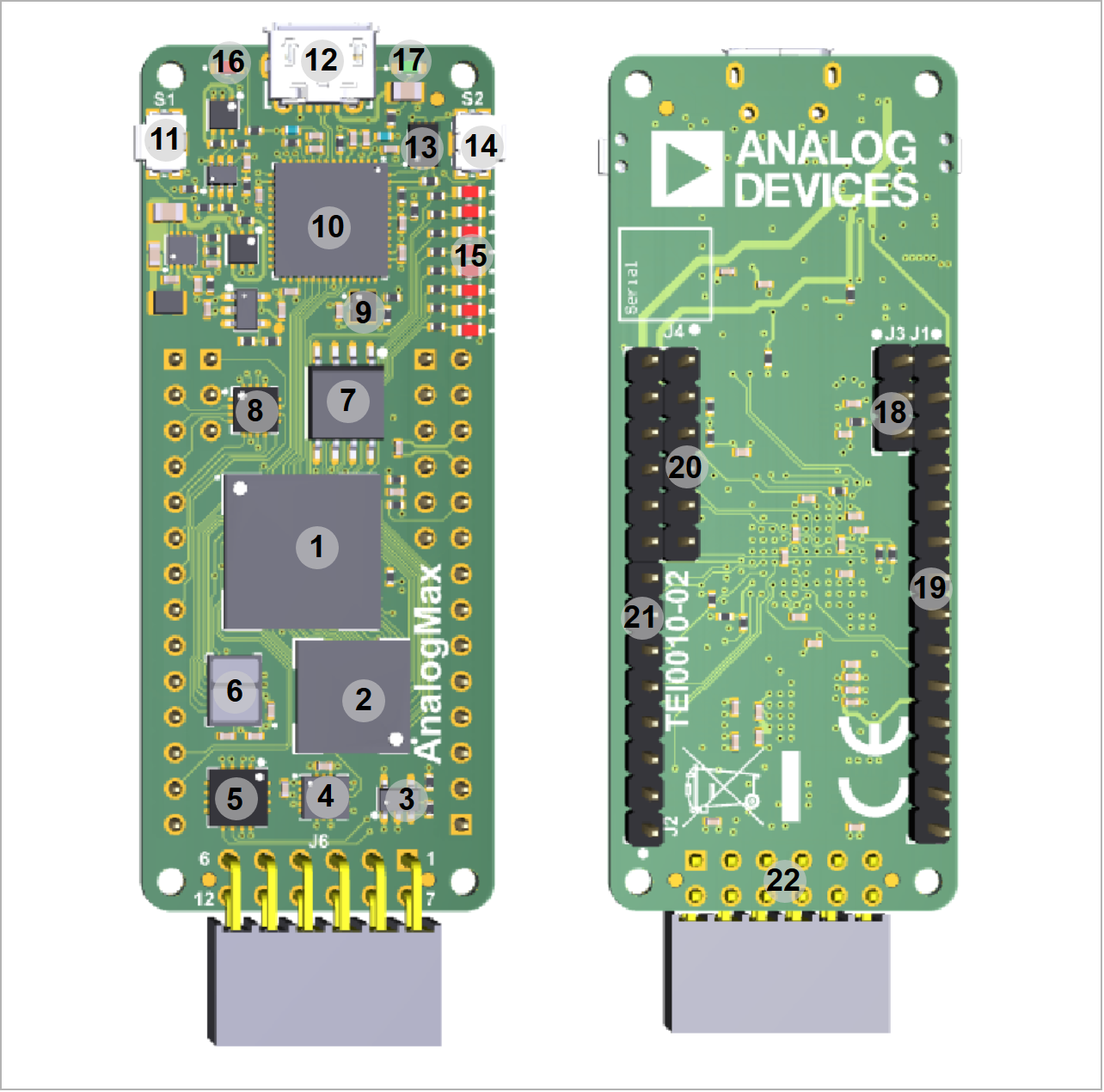
Intel MAX 10 10M08 FPGA SoC
- 8 MByte SDRAM
8 MByte QSPI Flash memory
- Onboard oscillator with 3 selectable frequencies
- Analog Devices ADXL362BCCZ ADXL362 MEMS 3-axis accelerometer
- Analog Devices ADT7320UCPZ T7320 temperature sensor
- Analog Devices ADPD188BI smoke detector
- Analog Devices AD5592RBCPZ 5592R ADC/DAC
- JTAG and UART over Micro USB2 connector
- 1x6 pin header for JTAG access to FPGA SoC
- 1x PMOD header providing 8 GPIOs
2x 14-pin headers (2,54 mm pitch) providing 22 GPIOs with 7 analog inputs as alternative function
- 1x 3-pin header providing 2 analog inputs or 1 GPIO
8x user LEDs
- 1x user push button
- 5.0V single power supply with on-board voltage regulators
- Size: 61.5 x 25 mm
...
| Scroll Title |
|---|
| anchor | Figure_OV_MC |
|---|
| title | Figure 2: TEI0010 main components |
|---|
|
| Scroll Ignore |
|---|
| draw.io Diagram |
|---|
| border | false |
|---|
| viewerToolbar | true |
|---|
| |
|---|
| fitWindow | false |
|---|
| diagramDisplayName | |
|---|
| lbox | true |
|---|
| revision | 2 |
|---|
| diagramName | TEI0010 main components |
|---|
| simpleViewer | false |
|---|
| width | |
|---|
| links | auto |
|---|
| tbstyle | hidden |
|---|
| diagramWidth | 642 |
|---|
|
|
| Scroll Only |
|---|
|
|
...
Initial Delivery State
| Scroll Title |
|---|
| anchor | Table_InitialOV_Delivery_StateIDS |
|---|
| title | Table 1: Initial delivery state of programmable devices on the module. |
|---|
|
| Scroll Table Layout |
|---|
| orientation | portrait |
|---|
| sortDirection | ASC |
|---|
| repeatTableHeaders | default |
|---|
| style | |
|---|
| widths | |
|---|
| sortByColumn | 1 |
|---|
| sortEnabled | false |
|---|
| cellHighlighting | true |
|---|
|
Storage device name | Content | Notes |
|---|
| Quad SPI Flash, U5 | DEMO Design | - | | FTDI chip configuration EEPROM, U9 | Programmed | - |
|
...
To get started with TEI0010 board, some basic signals are essential and are described in the following table:
| Scroll Title |
|---|
| anchor | Table_ControllOV_SignalsCS |
|---|
| title | Table 2: TEC0850 Control Signals |
|---|
|
| Scroll Table Layout |
|---|
| orientation | portrait |
|---|
| sortDirection | ASC |
|---|
| repeatTableHeaders | default |
|---|
| style | |
|---|
| widths | |
|---|
| sortByColumn | 1 |
|---|
| sortEnabled | false |
|---|
| cellHighlighting | true |
|---|
|
Control signal | Switch / Button / LED / Pin | Signal Schematic Names | Connected to | Functionality | Notes |
|---|
| MAX10 FPGA U1 JTAGEN | header J4, pin 2 | JTAGEN | MAX10 FPGA U1, bank 1B, pin E5 | high: MAX 10 JTAG enabled,
floating: MAX 10 JTAG disabled | switch the JTAG pins to user GPIO's if drive this pin to GND | | MAX10 FPGA U1 Reset | header J2, pin 10 | RESET | MAX10 FPGA U1, bank 8, pin E7 | low active reset line | also connected to Reset push button S1 | | Supply voltage indicator | Green LED D1 | 3.3V | DCDC DC-DC converter U4 | indicating 3.3V voltage level | - | | Configuration DONE indicator | Red LED D10 | CONF_DONE | MAX10 FPGA U1, bank 8, pin C5 | indicating FPGA configuration completed | ON: configuration completed, OFF: FPGA not configured | | Reset Push button | S1 | RESET | MAX10 FPGA U1, bank 8, pin E7 | low active logic | - | | User Push button | S2 | USER_BTN | MAX10 FPGA U1, bank 8, pin E6 | low active logic | available to user |
|
Boot Process
The FPGA configuration for Intel MAX 10 FPGAs can be stored through JTAG interface either in external configuration device (QSPI flash memory U5) or on the FPGA itself since the Intel MAX 10 FPGA offers non-volatile memory on chip. The FPGA configuration is loaded from the non-volatile memory when the board is powered up.
...
I/O signals of the FPGA SoC's I/O banks connected to the board's pin headers and connectors:
| Scroll Title |
|---|
| anchor | Table_OVSIP_I/O's |
|---|
| title | General overview of single ended I/O's on board headers |
|---|
|
| Scroll Table Layout |
|---|
| orientation | portrait |
|---|
| sortDirection | ASC |
|---|
| repeatTableHeaders | default |
|---|
| style | |
|---|
| widths | |
|---|
| sortByColumn | 1 |
|---|
| sortEnabled | false |
|---|
| cellHighlighting | true |
|---|
|
| Bank | Connector Designator | I/O Signal Count | Bank Voltage | Notes |
|---|
| 2 | J1 | 4 I/O's | 3.3V | - | | J6 | 8 I/O's | Pmod connector | | 5 | J1 | 2 I/O's | 3.3V | - | | J2 | 9 I/O's | 2 I/O's of bank 5 can be pulled-up to 3.3V (4K7 resistors) | | 1B | J4 | JTAG interface and 'JTAGEN' signal (5 I/O's) | 3.3V | JTAG enable signal (JTAGEN) on pin J4-2, switch between user I/O pins and JTAG pin functions | | J3 | 1 I/O | - |
|
...
Optionally 1x6 male pin header J4 can be fitted on board for access to the JTAG interface between FTDI and FPGA on board. The pin assignment of header J4 is shown on table below:
| Scroll Title |
|---|
| anchor | Table_OV_I/O'sSIP_JTAG |
|---|
| title | Optional JTAG pin header |
|---|
|
| Scroll Table Layout |
|---|
| orientation | portrait |
|---|
| sortDirection | ASC |
|---|
| repeatTableHeaders | default |
|---|
| style | |
|---|
| widths | |
|---|
| sortByColumn | 1 |
|---|
| sortEnabled | false |
|---|
| cellHighlighting | true |
|---|
|
| JTAG Signal | Pin on Header J4 | Note |
|---|
| TCK | 3 | - | | TDI | 5 | - | | TDO | 4 | - | | TMS | 6 | - | | JTAGEN | 2 | leave floating when use JTAG interface, otherwise signals on FPGA are GPIOs |
|
Micro-USB2 Connector
The Micro-USB2 connector J9 provides an interface to access to access the UART and JTAG functions via FTDI FT2232 chip. The use of this feature requires that USB driver is installed on your host PC.
The Digilent plug-in software and cable drivers must be installed on your machine for you to be able to use JTAG interface.
FPGA I/O banks
Table below contains the signals and interfaces of the FPGA banks connected to pins and peripherals of the board:
| Scroll Title |
|---|
| anchor | Table_OVSIP_FPGA-bank-I/O's |
|---|
| title | General overview of single ended FPGA bank I/O's |
|---|
|
| Scroll Table Layout |
|---|
| orientation | portrait |
|---|
| sortDirection | ASC |
|---|
| repeatTableHeaders | default |
|---|
| style | |
|---|
| widths | |
|---|
| sortByColumn | 1 |
|---|
| sortEnabled | false |
|---|
| cellHighlighting | true |
|---|
|
| Bank | I/O's Count | Connected to | Notes |
|---|
| 2 | 4 | 1x14 pin header, J1 | user GPIO's | | 8 | Pmod connector, J6 | user GPIO's | | 1 | clock oscillator, U7 | 12.0000 MHz reference clock input | | 1 | reference clock oscillator, U10 | reference clock input from adjustable oscillator U10 | | 1 | accelerometer IC, U11 | interrupt 1 line of Analog Devices MEMS accelerometer | | 5 | 9 | 1x14 pin header, J2 | 2 I/O's (D11, D12) of bank 5 can be pulled-up to 3.3V (4K7 resistors) with 1 I/O (D12_R) of same Bank bank and 1 I/O (D11_R) of bank 6 | | 1 | accelerometer IC, U11 | interrupt 2 line of Analog Devices MEMS accelerometer | | 1 | reference clock oscillator, U10 | control line to adjust oscillator adjustable with three steps frequencies of clock output | | 1 | temperature sensor IC, U8 | interrupt line of temperature thresholds | | 6 | 18 | 8 MByte SDRAM 166MHz, U2 | 16bit SDRAM memory interface | | 3 | 22 | 8 MByte SDRAM 166MHz, U2 | 16bit SDRAM memory interface | | 3 | SPI interface connected to IC U8, U11, U12 | SPI interface (MISO, MOSI, MCLK) for temperature sensor U8, 3-axis accelerometer U11 and ADC/DAC U12 | | 1 | temperature sensor IC, U8 | chip-select line for SPI interface | | 1 | accelerometer IC, U11 | chip-select line for SPI interface | | 1 | ADC/DAC IC , U12 | Synchronization data input frame synchronization line of ACD/DAC IC (active low control input) | | 1 | temperature sensor IC, U8 | interrupt line of critical temperature | | 1A | 8 | 1x14 pin headers J1 | 7 analog inputs or GPIO's, 1 pin analog reference voltage input | | 2 | pin headers J1 | 1 analog inputs or GPIO, 1 dedicated analog input | | smoke detector IC, U14 | SPI, I²C interface and GPIO's of smoke detector IC U14 | | 1B | 1 | pin headers J3 | 1 x GPIO | | 5 | FTDI FT2232H IC U3 (4 JTAG I/O's) and pin header J4 (5 I/O's) | 1B | 5 | pin header J4 | 4 I/O's JTAG interface and 1x 'JTAGEN' signal to switch the JTAG pins to user GPIO's if drive this pin to GND | | 8 | 8 | LEDs D2 ... D9 | Red user LEDs | | 6 | QSPI Flash memory, U5 | 6 pins Quad SPI interface, 2 of them pulled up as configuration pins during initialization | | 6 | FTDI FT2232H JTAG/UART adapter, U3 | 6 pins configurable as GPIO/UART or other serial interfaces | | 1 | Red LED, D10 | Configuration DONE Led (ON when configuration in progress, OFF when configuration is done) | | 1 | User button S2 | user configurable | | 1 | Reset button S1 and pin J2-10 | low active reset line for FPGA reconfiguration |
|
...
On-board serial configuration memory (U5) is provided by Winbond W74M64FVSSIQ with 64 MBit (8 MByte) storage capacity. This non volatile memory is used to store initial FPGA configuration via JTAG interface. The memory is connected to FPGA bank 1 via SPI interface.
| Scroll Title |
|---|
| anchor | Table_TSOBP_AMRSerialFlash |
|---|
| title | Quad SPI Flash memory interface |
|---|
|
| Scroll Table Layout |
|---|
| orientation | portrait |
|---|
| sortDirection | ASC |
|---|
| repeatTableHeaders | default |
|---|
| style | |
|---|
| widths | |
|---|
| sortByColumn | 1 |
|---|
| sortEnabled | false |
|---|
| cellHighlighting | true |
|---|
|
| Serial Memory U5 Pin | Signal Schematic Name | Connected to | Notes |
|---|
| Pin 1, CS | F_CS | FPGA bank 8, pin B3
| chip select | | Pin 6, CLK | F_CLK | FPGA bank 8, pin A3 | clock | | Pin 5, SI/IO0 | F_DI | FPGA bank 8, pin A2 | data in / out | | Pin 7, HOLD/IO3 | NSTATUS | FPGA bank 8, pin C4 | data in / out (configuration dual-purpose pin of FPGA) | | Pin 3, WP/IO2 | DEVCLRN | FPGA bank 8, pin B9 | data in / out (configuration dual-purpose pin of FPGA) | | Pin 2, SO/IO1 | F_DO | FPGA bank 8, pin B2 | data in / out |
|
...
The FPGA module is equipped with a Winbond W9864G6JT 64 MBit (8 MByte) SDRAM chip U2 in standard configuration, variants with 256 Mbit (32 MByte) memory density are also available. The SDRAM chip is connected to the FPGA bank 3 and 6 via 16-bit memory interface with 166MHz clock frequency and CL3 CAS latency.
| Scroll Title |
|---|
| anchor | Table_TSOBP_AMRSDRAM |
|---|
| title | 16bit SDRAM memory interface |
|---|
|
| Scroll Table Layout |
|---|
| orientation | portrait |
|---|
| sortDirection | ASC |
|---|
| repeatTableHeaders | default |
|---|
| style | |
|---|
| widths | |
|---|
| sortByColumn | 1 |
|---|
| sortEnabled | false |
|---|
| cellHighlighting | true |
|---|
|
| SDRAM I/O Signals | Signal Schematic Name | Connected to | Notes |
|---|
| Address inputs | A0 ... A13 | bank 3 | - | Bank address inputs
| BA0 / BA1 | bank 3 | - | | Data input/output | DQ0 ... DQ15 | bank 6 | - | | Data mask | DQM0 ... DQM1 | bank 6 | - | | Clock | CLK | bank 3 |
| | Control Signals | CS | bank 3 | Chip select | CKE | bank 3 | Clock enable | RAS | bank 3 | Row Address Strobe | CAS | bank 3 | Column Address Strobe | | WE | bank 3 | Write Enable |
|
...
The FTDI chip U3 converts signals from USB2 to a variety of standard serial and parallel interfaces. Refer to the FTDI data sheet to get information about the capacity of the FT2232H chip.
FTDI FT2232H chip is used in MPPSE mode for JTAG, 6 I/O's of Channel B are routed to FPGA bank 8 of the FPGA SoC and are usable for example as GPIOs, UART or other standard interfaces.
The configuration of FTDI FT2232H chip is pre-programmed on the EEPROM U9.
...
pre-programmed on the EEPROM U9.
Channel A of the FTDI IC chip is configured as JTAG interface (MPSSE) connected to the bank 1B of MAX10 FPGA U1.
Channel B can be used as UART Interface routed to the MAX10 FPGA U1, is routed via 6 I/O's of Channel B is routed to to bank 8 of MAX10 FPGA U1 and are usable for example as GPIOs and as FIFO, UART or other standard interfaces.
| Scroll Title |
|---|
| anchor | Table_TSOBP_AMRFTDI |
|---|
| title | FTDI chip interfaces and pins |
|---|
|
| Scroll Table Layout |
|---|
| orientation | portrait |
|---|
| sortDirection | ASC |
|---|
| repeatTableHeaders | default |
|---|
| style | |
|---|
| widths | |
|---|
| sortByColumn | 1 |
|---|
| sortEnabled | false |
|---|
| cellHighlighting | true |
|---|
|
| FTDI Chip U3 Pin | Signal Schematic Name | Connected to | Notes |
|---|
| Pin 12, ADBUS0 | TCK | FPGA bank 1B, pin G2
| JTAG interface | | Pin 13, ADBUS1 | TDI | FPGA bank 1B, pin F5 | | Pin 14, ADBUS2 | TDO | FPGA bank 1B, pin F6 | | Pin 15, ADBUS3 | TMS | FPGA bank 1B, pin G1 | | Pin 32, BDBUS0 | BDBUS0 | FPGA bank 8, pin A4 | user configurable | | Pin 33, BDBUS1 | BDBUS1 | FPGA bank 8, pin B4
| user configurable | | Pin 34, BDBUS2 | BDBUS2 | FPGA bank 8, pin B5 | user configurable | | Pin 35, BDBUS3 | BDBUS3 | FPGA bank 8, pin A6 | user configurable | | Pin 37, BDBUS4 | BDBUS4 | FPGA bank 8, pin B6
| user configurable | | Pin 38, BDBUS5 | BDBUS5 | FPGA bank 8, pin A7 | user configurable |
|
...
The ADC/DAC chip has following pin assignment with the FPGA and the board pin-headers, where its I/O pins are available:
| Scroll Title |
|---|
| anchor | Table_TSOBP_AMRADC/DAC |
|---|
| title | ADC/DAC interfaces and pins |
|---|
|
| Scroll Table Layout |
|---|
| orientation | portrait |
|---|
| sortDirection | ASC |
|---|
| repeatTableHeaders | default |
|---|
| style | |
|---|
| widths | |
|---|
| sortByColumn | 1 |
|---|
| sortEnabled | false |
|---|
| cellHighlighting | true |
|---|
|
ADC/DAC U12 pin | Signal Schematic Name | Connected to | Notes |
|---|
| Pin 2, I/O0 | AIN0 | header J1, pin 2
| I/O pins configurable
as DAC output, ADC input
or digital GPIOs | | Pin 3, I/O1 | AIN1 | header J1, pin 3
| | Pin 4, I/O2 | AIN2 | header J1, pin 4
| | Pin 5, I/O3 | AIN3 | header J1, pin 5 | | Pin 8, I/O4 | AIN4 | header J1, pin 6
| | Pin 9, I/O5 | AIN5 | header J1, pin 7
| | Pin 10, I/O6 | AIN6 | header J1, pin 8 | | Pin 11, I/O7 | AIN7 | header J3, pin 1 | | Pin 6, VREF | AREF | header J1, pin 1 | Analog I/O's reference voltage.
Note: Internal reference voltage of
2.5V is available on this pin when enabled,
else extern analog reference voltage (range: 1V ... VDD)
has to be applied on this pin. | | Pin 15, nRESET | ADDA_RSTN | FPGA bank 8, pin D6 | IC active low reset pin | | Pin 16, nSYNC | ADDA_SYNC | FPGA bank 3, pin J5 | Frame synchronization signal, data is transferred in
on the falling edge of the next 16 clock cycles. | | Pin 14, SCLK | MCLK | FPGA bank 3, pin J7 | serial clock input | | Pin 13, SDI | MOSI | FPGA bank 3, pin K5 | data input | | Pin 7, SDO | MISO | FPGA bank 3, pin J6 | data output |
|
...
On the TEI0010 board there is a 3-axis MEMS accelerometer present provided by Analog Devices ADXL362. This accelerometer with 12-bit internal ADC resolution offers many functions to detect motion and has also a temperature sensor integrated. It also has a FIFO buffer for storing output data. The sensor is connected to the FPGA through SPI interface and two interrupt lines.
| Scroll Title |
|---|
| anchor | Table_TSOBP_AMRAccelorometer |
|---|
| title | 3-axis accelerometer interfaces and pins |
|---|
|
| Scroll Table Layout |
|---|
| orientation | portrait |
|---|
| sortDirection | ASC |
|---|
| repeatTableHeaders | default |
|---|
| style | |
|---|
| widths | |
|---|
| sortByColumn | 1 |
|---|
| sortEnabled | false |
|---|
| cellHighlighting | true |
|---|
|
| Accelerometer U11 Pin | Signal Schematic Name | Connected to | Notes |
|---|
| Pin 11, INT1 | MEMS_INT1 | FPGA bank 2, pin L2
| Interrupt lines | | Pin 9, INT2 | MEMS_INT2 | FPGA bank 5, pin J9 | | Pin 6, MOSI | MOSI | FPGA bank 3, pin K5 | SPI interface | | Pin 7, MISO | MISO | FPGA bank 3, pin J6 | | Pin 8, nCS | MEMS_CS | FPGA bank 3, pin L5 | | Pin 4, SCLK | MCLK | FPGA bank 3, pin J7 |
|
...
The TEI0010 board is equipped with the Analog Devices ADPD188BI optical module for smoke detection. The smoke detector IC has two digital GPIO's, I²C and SPI serial bus as interface for the data output and as control and configuration interface. The smoke detector IC has an integrated 128-byte FIFO buffer for conversed analog values. The values of the internal 14-bit ADC are enhanced for more precision to 20 bits, on 32-bit output register averaged ADC values with a precision of 27 bits are available. For configurable interrupts and timing signals etc., the smoke detector IC offers two GPIO's, which are routed to the FPGA.
| Scroll Title |
|---|
| anchor | Table_TSOBP_AMRSmokeDetector |
|---|
| title | Smoke detector interfaces and pins |
|---|
|
| Scroll Table Layout |
|---|
| orientation | portrait |
|---|
| sortDirection | ASC |
|---|
| repeatTableHeaders | default |
|---|
| style | |
|---|
| widths | |
|---|
| sortByColumn | 1 |
|---|
| sortEnabled | false |
|---|
| cellHighlighting | true |
|---|
|
Smoke Detector U14 pin | Signal Schematic Name | Connected to | Notes |
|---|
| Pin 12, SCL | IOM_SCL | FPGA bank 1A, pin F1
| I²C interface | | Pin 13, SDA | IOM_SDA | FPGA bank 1A, pin E1
| | Pin 18, SCLK | ADP_SCK | FPGA bank 1A, pin C2
| SPI interface | | Pin 17, MOSI | ADP_MOSI | FPGA bank 1A, pin C1 | | Pin 16, MISO | ADP_MISO | FPGA bank 1A, pin E4
| | Pin 19, CSB | ADP_CS | FPGA bank 1A, pin B1
| | Pin 14, GPIO0 | IOM_GPIO0 | FPGA bank 1A, pin E3 | GPIO's | | Pin 15, GPIO1 | IOM_GPIO1 | FPGA bank 1A, pin D1 |
|
...
The TEI0010 is equipped with the Analog Devices ADT7320 temperature sensor with SPI interface. The temperature sensor offers a temperature value resolution of 16-bit and high accuracy in temperature measuring. The temperature sensor has two interrupt lines which are configurable to be triggered at a programmable undertemperature/overtemperature or critical temperature value.
| Scroll Title |
|---|
| anchor | Table_TSOBP_AMRTempSensor |
|---|
| title | Temperature sensor interfaces and pins |
|---|
|
| Scroll Table Layout |
|---|
| orientation | portrait |
|---|
| sortDirection | ASC |
|---|
| repeatTableHeaders | default |
|---|
| style | |
|---|
| widths | |
|---|
| sortByColumn | 1 |
|---|
| sortEnabled | false |
|---|
| cellHighlighting | true |
|---|
|
Temperature Sensor U8 pin | Signal Schematic Name | Connected to | Notes |
|---|
| Pin 1, SCLK | MCLK | FPGA bank 3, pin J7
| SPI interface | | Pin 3, DIN | MOSI | FPGA bank 3, pin K5
| | Pin 2, DOUT | MISO | FPGA bank 3, pin J6
| | Pin 4, nCS | TEMP_CS | FPGA bank 3, pin L4 | | Pin 9, INT | TEMP_INT | FPGA bank 5, pin L13
| Interrupt lines | | Pin 10, CT | TEMP_CT | FPGA bank 3, pin N12 |
|
...
The FPGA SoC module has following reference clocking signals provided by on-board oscillators:
| Scroll Title |
|---|
| anchor | Table_TSOBP_AMROscillators |
|---|
| title | Clock sources overview |
|---|
|
| Scroll Table Layout |
|---|
| orientation | portrait |
|---|
| sortDirection | ASC |
|---|
| repeatTableHeaders | default |
|---|
| style | |
|---|
| widths | |
|---|
| sortByColumn | 1 |
|---|
| sortEnabled | false |
|---|
| cellHighlighting | true |
|---|
|
| Clock Source | Schematic Name | Frequency | Clock Input Destination | Notes |
|---|
| Microchip MEMS Oscillator DSC6011ME2A, U7 | CLK12M | 12.0000MHz | FTDI FT2232 U3, pin 3; FPGA SoC bank 2, pin H6 | - | | Adjustable Oscillator LTC1799CS5, U10 | OSC_CLK | 8.33MHz / 833.33KHz / 83.33KHz | FPGA SoC bank 2, pin G5 | Frequency is set with signal 'OSC_DIV', which is tied
to FPGA bank 5, pin H9. Following settings are available: FPGA pin H9 ('OSC_DIV') open drain: 8.33MHz
FPGA pin H9 ('OSC_DIV') open drain: 833.33KHz
FPGA pin H9 ('OSC_DIV') pulled to 3.3V: 83.33KHz |
|
...
There are 10 LEDs fitted on the FPGA module board. The LEDs are user configurable to indicate for example any system status.
| Scroll Title |
|---|
| anchor | Table_TSOBP_AMRLEDs |
|---|
| title | LEDs of the module |
|---|
|
| Scroll Table Layout |
|---|
| orientation | portrait |
|---|
| sortDirection | ASC |
|---|
| repeatTableHeaders | default |
|---|
| style | |
|---|
| widths | |
|---|
| sortByColumn | 1 |
|---|
| sortEnabled | false |
|---|
| cellHighlighting | true |
|---|
|
| LED | Color | Signal Schematic Name | FPGA | Notes |
|---|
| D1 | Green | 3.3V | - | Indicating 3.3V board supply voltage | | D2 | Red | 'LED1' | bank 8, pin D8 | user | | D3 | Red | 'LED2' | bank 8, pin A8 | user | | D4 | Red | 'LED3' | bank 8, pin A9 | user | | D5 | Red | 'LED4' | bank 8, pin C9 | user | | D6 | Red | 'LED5' | bank 8, pin A10 | user | | D7 | Red | 'LED6' | bank 8, pin B10 | user | | D8 | Red | 'LED7' | bank 8, pin A11 | user | | D9 | Red | 'LED8' | bank 8, pin C10 | user | | D10 | Red | 'CONF_DONE' | bank 8, pin C5 | indication configuration is DONE when LED is off |
|
...
The FPGA module is equipped with two push buttons S1 and S2:
| Scroll Title |
|---|
| anchor | Table_TSOBP_AMRPushButtons |
|---|
| title | Push buttons of the module |
|---|
|
| Scroll Table Layout |
|---|
| orientation | portrait |
|---|
| sortDirection | ASC |
|---|
| repeatTableHeaders | default |
|---|
| style | |
|---|
| widths | |
|---|
| sortByColumn | 1 |
|---|
| sortEnabled | false |
|---|
| cellHighlighting | true |
|---|
|
| Button | Signal Schematic Name | FPGA | Notes |
|---|
| S1 | 'USER_BTN' | bank 8, pin E6 | user configurable | | S2 | 'RESET' | bank 8, pin E7 | FPGA reset |
|
...
| Scroll Title |
|---|
| anchor | Figure_PWR_PD |
|---|
| title | Figure x: Power Distribution |
|---|
|
| Scroll Ignore |
|---|
| draw.io Diagram |
|---|
| border | false |
|---|
| viewerToolbar | true |
|---|
| |
|---|
| fitWindow | false |
|---|
| diagramDisplayName | |
|---|
| lbox | true |
|---|
| revision | 1 |
|---|
| diagramName | TEI0010 power distribution dependencies |
|---|
| simpleViewer | false |
|---|
| width | |
|---|
| links | auto |
|---|
| tbstyle | hidden |
|---|
| diagramWidth | 641 |
|---|
|
|
| Scroll Only |
|---|
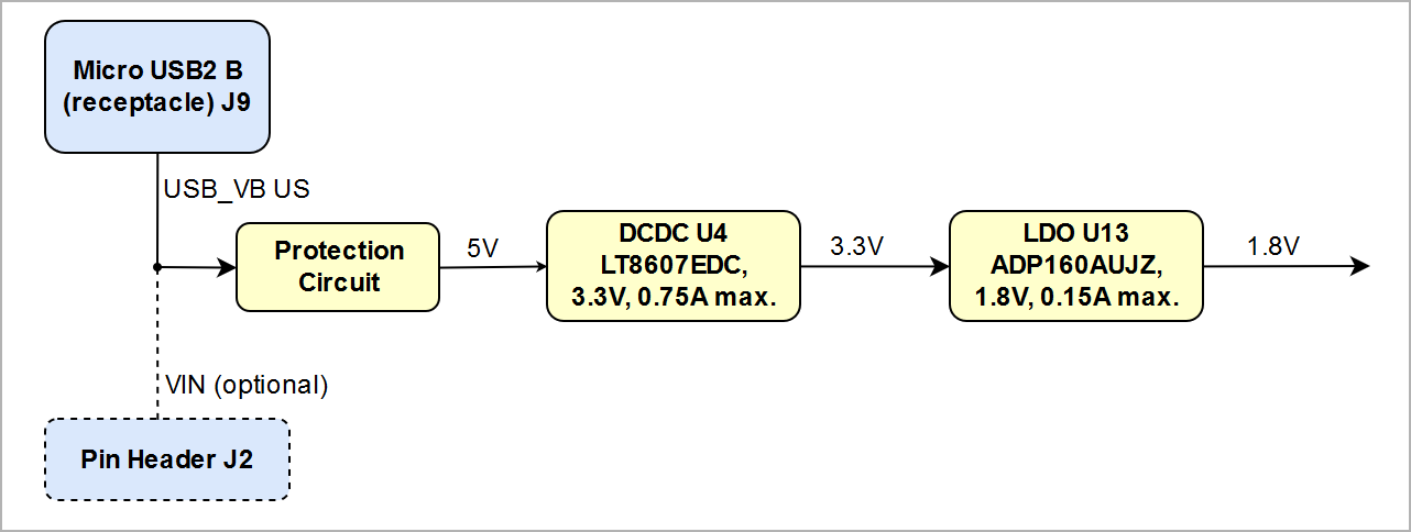 Image Added Image Added
|
|
Power Consumption
| Scroll Title |
|---|
| anchor | Table_TSPWR_AMRPC |
|---|
| title | Module power consumption |
|---|
|
| Scroll Table Layout |
|---|
| orientation | portrait |
|---|
| sortDirection | ASC |
|---|
| repeatTableHeaders | default |
|---|
| style | |
|---|
| widths | |
|---|
| sortByColumn | 1 |
|---|
| sortEnabled | false |
|---|
| cellHighlighting | true |
|---|
|
| FPGA | Design | Typical Power, 25C ambient |
|---|
| Intel MAX 10 10M08 FPGA SoC | Not configured | TBD* |
|
...
Power Rails
| Scroll Title |
|---|
| anchor | Table_TSPWR_AMRPR |
|---|
| title | Connector power pin description |
|---|
|
| Scroll Table Layout |
|---|
| orientation | portrait |
|---|
| sortDirection | ASC |
|---|
| repeatTableHeaders | default |
|---|
| style | |
|---|
| widths | |
|---|
| sortByColumn | 1 |
|---|
| sortEnabled | false |
|---|
| cellHighlighting | true |
|---|
|
| Connector Designator | VCC / VCCIO Schematic Name | Voltage | Direction | Pins | Notes |
|---|
| J2 | 5V | 5.0V | Out | Pin 14 | - | | VIN | 5.0V | In | Pin 13 | - | | 3.3V | 3.3V | Out | Pin 12 | - | | J6 | 3.3V | 3.3V | Out | Pin 6, 12 | - | | J9 | USB_VBUS | 5.0V | In | Pin 1 | - |
|
Bank Voltages
| Scroll Title |
|---|
| anchor | Table_TSPWR_AMRBV |
|---|
| title | FPGA SoC VCCO bank voltages |
|---|
|
| Scroll Table Layout |
|---|
| orientation | portrait |
|---|
| sortDirection | ASC |
|---|
| repeatTableHeaders | default |
|---|
| style | |
|---|
| widths | |
|---|
| sortByColumn | 1 |
|---|
| sortEnabled | false |
|---|
| cellHighlighting | true |
|---|
|
| Voltage | |
|---|
| 2 | 3.3V | all bank voltages fixed | | 3 | 3.3V | | 5 | 3.3V | | 6 | 3.3V | | 1A | 1.8V | | 1B | 3.3V | | 8 | 3.3V |
|
...
| Scroll Title |
|---|
| anchor | Table_TS_AMR |
|---|
| title | Module absolute maximum ratings. |
|---|
|
| Scroll Table Layout |
|---|
| orientation | portrait |
|---|
| sortDirection | ASC |
|---|
| repeatTableHeaders | default |
|---|
| style | |
|---|
| widths | |
|---|
| sortByColumn | 1 |
|---|
| sortEnabled | false |
|---|
| cellHighlighting | true |
|---|
|
Parameter | Min | Max | Units | Reference document |
|---|
VIN supply voltage (5.0V nominal) | 4.75 | 5.25 | V | USB2.0 VBUS specification | | I/O Input voltage for FPGA I/O bank | -0.5 | 4.12 | V | Intel MAX 10 datasheet | | Voltage on ADC/DAC IC U12 pins | -0.3 | 3.6.0 | V | EP53A7HQI AD5592R datasheet | | I/O Input voltage for FPGA I/O bankAnalog reference voltage on IC U12 | -0.53 | 43.126 | V | Intel MAX 10 AD5592R datasheet | Storage Temperature | -40 | +90 | °C | LED R6C-AL1M2VY/3T datasheet |
|
...
| Scroll Title |
|---|
| anchor | Table_TS_AMRROC |
|---|
| title | Recommended Operating Conditions. |
|---|
|
| Scroll Table Layout |
|---|
| orientation | portrait |
|---|
| sortDirection | ASC |
|---|
| repeatTableHeaders | default |
|---|
| style | |
|---|
| widths | |
|---|
| sortByColumn | 1 |
|---|
| sortEnabled | false |
|---|
| cellHighlighting | true |
|---|
|
| Parameter | Min | Max | Units | Reference document |
|---|
| VIN supply voltage (5.0V nominal) | 4.75 | 5.25 | V | same as USB-USB2.0 VBUS specification | | I/O Input voltage for FPGA I/O bank | –0.5 | 3.6 | V | Intel MAX 10 datasheet | | Voltage on ADC/DAC IC U12 pins | 0 | 3.3 | V | AD5592R datasheet | | Analog reference voltage on IC U12 | 1 | 3.3 | V | AD5592R datasheet | | Operating temperature range | 0 | +70 | °C | Winbond datasheet W9864G6GT |
|
Physical Dimensions
| Scroll Title |
|---|
| anchor | Figure_TS_PD |
|---|
| title | Physical dimensions drawing |
|---|
|
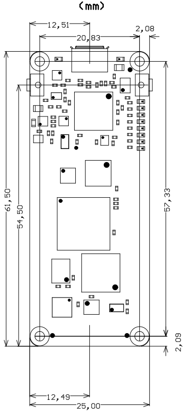 Image Added Image Added 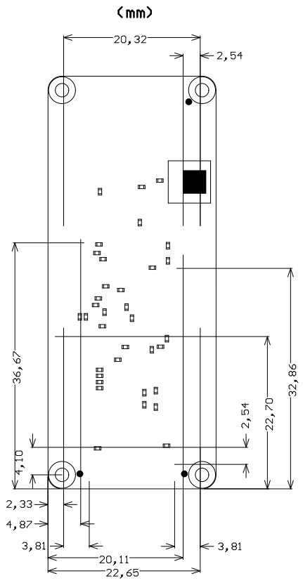 Image Added Image Added |
Variants Currently In Production
...
| Scroll Title |
|---|
| anchor | Table_VCP_SO |
|---|
| title | Trenz Electronic Shop Overview |
|---|
|
| Scroll Table Layout |
|---|
| orientation | portrait |
|---|
| sortDirection | ASC |
|---|
| repeatTableHeaders | default |
|---|
| style | |
|---|
| widths | |
|---|
| sortByColumn | 1 |
|---|
| sortEnabled | false |
|---|
| cellHighlighting | true |
|---|
|
|
Revision History
Hardware Revision History
| Scroll Title |
|---|
| anchor | Table_RH_HRH |
|---|
| title | Hardware Revision History |
|---|
|
| Scroll Table Layout |
|---|
| orientation | portrait |
|---|
| sortDirection | ASC |
|---|
| repeatTableHeaders | default |
|---|
| style | |
|---|
| widths | |
|---|
| sortByColumn | 1 |
|---|
| sortEnabled | false |
|---|
| cellHighlighting | true |
|---|
|
| Date | Revision | Notes | PCN | Documentation Link |
|---|
| - | 02 | First Production Release | - | TEI0010-02 | | - | 01 | Prototypes | - | TEI0010-01 |
|
Document Change History
| Page properties |
|---|
|
- Note this list must be only updated, if the document is online on public doc!
- It's semi automatically, so do following
Add new row below first Copy "Page Information Macro(date)" Macro-Preview, Metadata Version number, Author Name and description to the empty row. Important Revision number must be the same as the Wiki document revision number Update Metadata = "Page Information Macro (current-version)" Preview+1 and add Author and change description. --> this point is will be deleted on newer pdf export template - Metadata is only used of compatibility of older exports
|
...