Page History
| Table of Contents |
|---|
Overview
This demo provides an example on how to use the communication interface provided in the modules firmware
to setup the pre-amplification gain and trigger an ADC measurement. This measurement is converted to show
its it's value over time, and Fourier transformed, showing its it's Fast Fourier Transformation / frequency spectrum.
The download of the demo The download contains the demo in a separate folder and , a folder with Setup Notebooks, the FPGA Design file and the related wiki pages in pdf format.
The demo consist of two files, one is the notebook Notebook which contains the GUI and the other is a code module,
containing the functional analytical part of the demo. These files must be in the same folder when running the demo.
The modules ADC is controlled via the Intel Max 10 FPGA. In shipment condition, the FPGA is programmed with
with the necessary FPGA Design to run this demo.
Using the demo
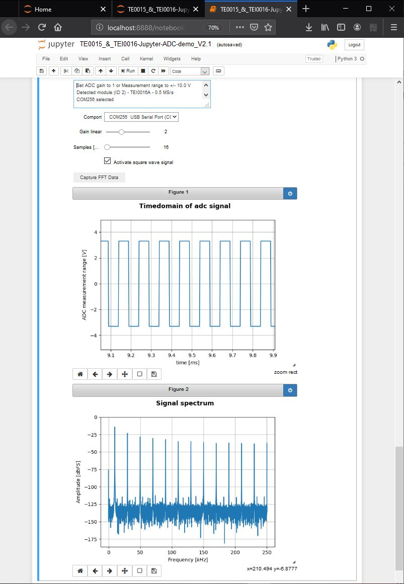
This demo is designed with the focus of capturing signals. Therefore the module works like a storage
oscilloscope. After a trigger event, the module saves 1 million samples of ADC measurement in its SDRAM.
The demo scans for existing comports in its initialisation phase. So the module needs to be connected
to the computer prior to running the demo.
When this demo runs, it displays a graphical user interface, setup the comport, the demo automatically selects
the module. After this, the demo and the module can communicate.
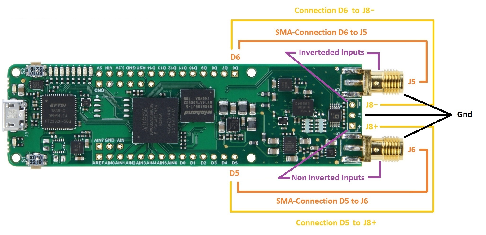
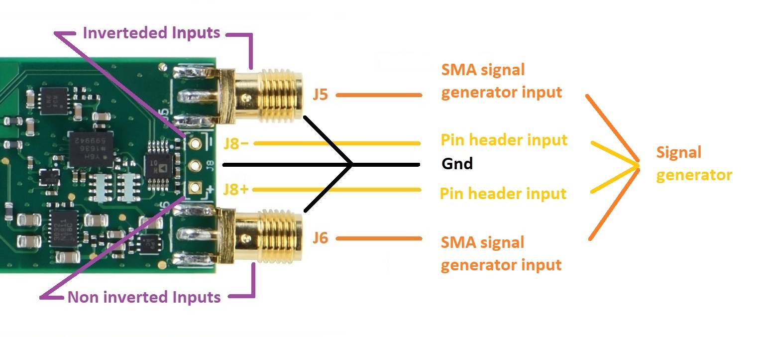
The module offers a Non inverted input and an inverted input. The inputs is accessible through either
a SMA connection or a breakout connection.
Inverted inputs are J5 and -J8
Non inverted inputs are J6 and +J8
Now supply a signal to the inputs.
An other option is to use the modules square wave signal output. Connect the digital outputs D5 and D6 to
the inputs as you like and activate the signal through the checkbox.
Be careful, do not shorten the outputs D5 or D6 to ground.
One can set up a pre amplification gain of the input signal and the amount of samples to be processed.
By pressing the button Capture FFT data, the input signal will be plotted and shown.
Communicating with module:
To communicate with the module, a serial comport port with a speed set to 115200 bits needs to be opened.
Commands consists of a single character in UTF-8 encoding.
It is good practice to communication with the module following these steps:
- Open a serial comport
- Clear the PCs serial comport input buffer of the opened comport
- Send the desired commands, each one in a single write operation to the comport
- Close the serial comport as soon as possible
These steps apply also for read operations.
Using the ADC for high speed consecutive measurements
The module provides a method to gather highly accurate consecutive ADC measurements in a single event.
In this mode of operation, one mega sample of ADC values are performed and stored inside the modules
SD-RAM.
The following step should be taken in this mode:
- Open a serial comport
- Send the command "1", "2", "4" or "8" for the ADC pre-amplification
- Send the command "t" to trigger the consecutive measurement.
(The module always measures 1 MSample of data into its SD-RAM) - Clear the PCs serial comport input buffer of the opened comport
- Send the command "+" or "*"to the module, it then transmits 128 or 16384 Samples of ADC values
- Read the amount of ADC values in one chunk of 128 or 16384 samples from the PCs serial input buffer
(Otherwise there is a high possibility of a misalignment of nibbles) - Repeat the reading of chunks to a maximum of 1 mega sample
- Close the comport
After a trigger event, the one mega sample of data is stored until your retrigger. So processing the data can
be done for each chunk individually or the whole one mega sample.
Information to convert the RAW ADC data into standard integer values.
Module TEI0015 - AD4003BCPZ-RL7
Resolution: 18-bit in 5 nibbles
Maximum sampling rate: 2 MSPS
Order of Values:
...
The wiki page "Installation guide for Jupyter", available via the superior page, describes how to run Jupyter, install this Notebooks dependencies, open a Notebook and execute it.
Picture of the Notebook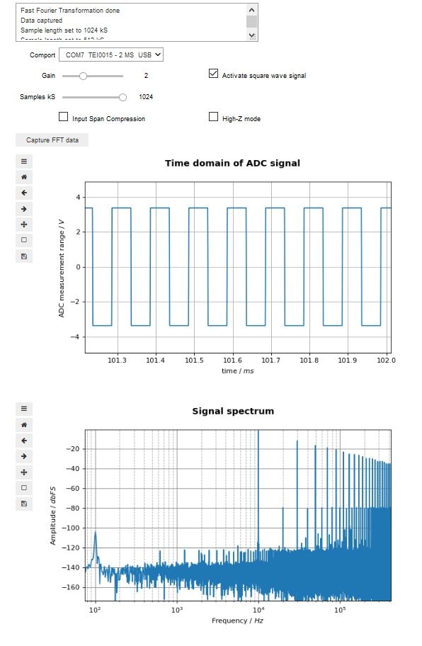
GUI elements
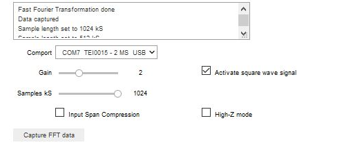
Drop-down List "Comport" :
- COM-port list for selecting a COM-port.
Listed are the port, the modules name and its USB ID
During notebook initialization, ports are scanned
Slider "Gain" :
Select the pre-amplification gain of the module
Different values in dependency to the module
Slider "Samples kS" :
Slider to set the samples to evaluate
Range is from 16 kS to 1024 kS
Check box "Activate square wave signal" :
Activates the modules square wave generator
10 kHz, +3.3V, 50% duty cycle, signal available with and without 180° phase shift
Check box "Input span compression" :
Mode of the modules ADC in which it's reference voltage is reduced to 80% to give head room in case the supply voltage is near to the reference voltage
Not available on all modules, greyed out / deactivated for these modules
Check box "High-Z mode" :
Mode of the modules ADC in which it reduces its current consumption. Not applicable to signal greater then 100 kHz
Not available on all modules, greyed out / deactivated for these modules
Button "Capture FFT data" :
Re-applies the appointed GUI values and features to the module and triggers a signal measurement followed by the data conversion and plotting
Using the demo
This demo is designed with the focus of capturing signals. Therefore the module works like a storage oscilloscope.
For every trigger event, the module saves 1 million samples of ADC measurement in its SDRAM. In the Notebook, the user just selects which amount of the data are to be used for the evaluation.
Module and host pc setup
The Notebook displays a graphical user interface in its running state, for setting up the comport, sample parameters, gain and module specific features. The following list describes the setup steps necessary prior to executing the Notebook:
- Connect the module to the host pc
- Apply a signal to the modules inputs:
Either via SMA- or via Pin Header- connection,
it is sufficient to use only one of the differential inputs,
but for the best results, apply the signal via both differential inputs
(Connection diagrams are in the next chapter) - Connect the module to the host pc
- Open Jupyter and navigate to the Notebook.
- Place the mouse cursor into the Notebooks cell via left click
- Run the Note by pressing the Run button
(The demo scans for existing comports in its initialisation phase. So the module needs to be connected to the computer prior to running the demo) - Enjoy !
Connecting the input signal
Connecting the square wave generator to the modules inputs
Appling a signal to the modules inputs
The layout of the ADC circuit is further described in the Analog Devices circuit note CN-0385.
Module TEI0016 - ADAQ7988 / ADAQ7980
Resolution: 16-bit in 4 nibbles
Maximum sampling rate: 0.5 MSps / 1 MSps
Order of Values:
...
Overview
Content Tools