...
The Trenz Electronic TEP0006 is a an Ultra96 LS Expansion to Pmod adapter.
...
- On Board:
- 4x Voltage Level Translators
- 2x Voltag Voltage Regulators
- Interface:
- 1x Ultra96 LS Expansion Header (40 Pins)
- 3x Pmod Connectors
- 3x Jumpers
- Power:
- Dimension:
...
| Scroll Title |
|---|
| anchor | Figure_OV_BD |
|---|
| title | TEP0006 block diagram |
|---|
|
| Scroll Ignore |
|---|
| draw.io Diagram |
|---|
| border | false |
|---|
| viewerToolbar | true |
|---|
| |
|---|
| fitWindow | false |
|---|
| diagramDisplayName | |
|---|
| lbox | true |
|---|
| revision | 57 |
|---|
| diagramName | TEP0006_OV_BD |
|---|
| simpleViewer | false |
|---|
| width | |
|---|
| links | auto |
|---|
| tbstyle | hidden |
|---|
| diagramWidth | 641 |
|---|
|
|
| Scroll Only |
|---|
 Image Modified Image Modified
|
|
Main Components
...
| Scroll Title |
|---|
| anchor | Figure_OV_MC |
|---|
| title | TEP0006 Main Components |
|---|
|
| Scroll Ignore |
|---|
| draw.io Diagram |
|---|
| border | false |
|---|
| viewerToolbar | true |
|---|
| |
|---|
| fitWindow | false |
|---|
| diagramDisplayName | |
|---|
| lbox | true |
|---|
| revision | 35 |
|---|
| diagramName | TEP0006_OV_MC |
|---|
| simpleViewer | false |
|---|
| width | |
|---|
| links | auto |
|---|
| tbstyle | hidden |
|---|
| diagramWidth | 641 |
|---|
|
|
| Scroll Only |
|---|
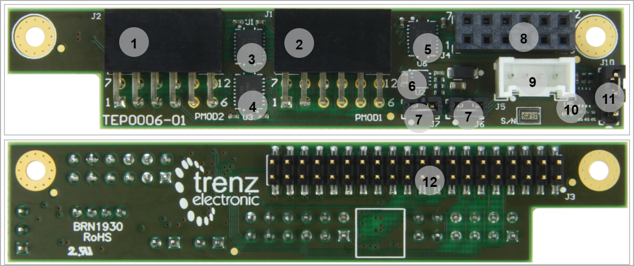 Image Modified Image Modified
|
|
- PMod 2x6 Host Socke (PMOD 2) ,J2
- PMod 2x6 Host Socke (PMOD 2) ,J1
- Level Translator (HP_GPIO[0..7]) ,U1
- Level Translator (HP_GPIO[8..15]),U3
- Level Translator PMOD(SPI),U6
- Linear Voltage Regulator,U2
- Jumper,J6-J7
- PMod 2x6 Host Socke (SPI),J4
- GROVE,J5
- Level Translator (GROVE) ,U5
- Jumper (Voltage select ),J10
- SMD Ultra96 LS Expansion Header (40 Pos. (LS Expansion ),J3
Initial Delivery State
...
Low Speed Expansion Connector
The SMD Header J3 has 40 pin (20x2) and it is compatible with Ultra96 LS Expansion Connector. You can find General information about GPIO connection to the LS Expansion connector :in the following table.
| Scroll Title |
|---|
| anchor | Table_SIP_Ultra96 |
|---|
| title | Ultra96 LS Expansion information |
|---|
|
| Scroll Table Layout |
|---|
| orientation | portrait |
|---|
| sortDirection | ASC |
|---|
| repeatTableHeaders | default |
|---|
| style | |
|---|
| widths | |
|---|
| sortByColumn | 1 |
|---|
| sortEnabled | false |
|---|
| cellHighlighting | true |
|---|
|
| Schematic | Connected to | Notes |
|---|
| HD_GPIO0...7 | Level Translator HP_GPIO[0...7], U1GPIO | GPIO0...7 | HD_GPIO8...15 | Level Translator HP_GPIO[8...15], U3 | GPIOGPIO8...15 | MIO36 -...37 | Level Translator PMOD(SPI)GPIO0-GPIO1 | PS_GPIO_0...1 | | MIO38, MIO41...43 | Level Translator PMOD(SPI) | SPI | | VCC_PSAUX | Level Translator, U1-U3-U5-U6 Voltage Regulator, U2 | 1.8 V nPOK | | 5V | Voltage Regulator, U2 Jumper, J10 | Vin Pull up Voltage |
|
Pmod Connectors
The TEP0006 is equipped with three Pmod connectors. Pmod Connectors are the expanded outputs from Ultra96 Board.
| Scroll Title |
|---|
| anchor | Table_SIP_Pmod |
|---|
| title | Pmod Connectors information |
|---|
|
| Scroll Table Layout |
|---|
| orientation | portrait |
|---|
| sortDirection | ASC |
|---|
| repeatTableHeaders | default |
|---|
| style | |
|---|
| widths | |
|---|
| sortByColumn | 1 |
|---|
| sortEnabled | false |
|---|
| cellHighlighting | true |
|---|
|
Pin | Connected to | Notes |
|---|
| Pmod 1, J1 | Pmod 2, J2 | Pmod SPI, J4 |
|---|
Notes |
|---|
| 1 | PMOD_HD-GPIO0 | PMOD_HD-GPIO8 | SS |
| | 2 | PMOD_HD-GPIO1 | PMOD_HD-GPIO9 | MOSI |
| | 3 | PMOD_HD-GPIO2 | PMOD_HD-GPIO10 | MISO |
| | 4 | PMOD_HD-GPIO3 | PMOD_HD-GPIO11 | SCK |
| | 5 | GND | GND | GND |
| | 6 | 3.3 V | 3.3 V | 3.3 V |
| | 7 | PMOD_HD-GPIO4 | PMOD_HD-GPIO12 | INIT |
| | 8 | PMOD_HD-GPIO5 | PMOD_HD-GPIO13 | RESET |
| | 9 | PMOD_HD-GPIO6 | PMOD_HD-GPIO14 | Not Connected |
| | 10 | PMOD_HD-GPIO7 | PMOD_HD-GPIO15 | Not Connected |
| | 11 | GND | GND | GND |
| | 12 | 3.3 V | 3.3 V | 3.3 V |
|
|
Jumpers
| Scroll Title |
|---|
| anchor | Table_SIP_Pmod |
|---|
| title | Pmod Connectors information |
|---|
|
| Scroll Table Layout |
|---|
| orientation | portrait |
|---|
| sortDirection | ASC |
|---|
| repeatTableHeaders | default |
|---|
| style | |
|---|
| widths | |
|---|
| sortByColumn | 1 |
|---|
| sortEnabled | false |
|---|
| cellHighlighting | true |
|---|
|
| Designator | Functionality | Connection Between | Notes |
|---|
J6 | HD_GPIO_15 VCC_PSAUX | J7 | Level Translator U3 and U5 | If you install the jumper HD_GPIO_15 | VCC_PSAUX will be driven through Level Translator (U5) and Grove (J5) otherwise it goes to Level Translator (U3). | | J7 | HD_GPIO_11 | Level Translator U3 and U5 | If you put the jumper HD_GPIO_11 will be driven through Level Translator (U5) and Grove (J5) otherwise it goes to Level Translator (U3). | | J10 | Voltage select | J10 | Voltage select | SDA | 5 V, 3.3 V SDA can be either 5 V or 3.3 V | Pull up Voltage |
|
On-board Peripherals
| Page properties |
|---|
|
Notes : - add subsection for every component which is important for design, for example:
- Two 100 Mbit Ethernet Transciever PHY
- USB PHY
- Programmable Clock Generator
- Oscillators
- eMMCs
- RTC
- FTDI
- ...
- DIP-Switches
- Buttons
- LEDs
|
...
| Page properties |
|---|
|
In 'Power and Power-on Sequence' section there are three important digrams which must be drawn: - Power on-sequence
- Power distribution
- Voltage monitoring circuit
|
Power Supply
Power supply with minimum current capability of 1 A for system startup is recommendedis supplied by Ultra96 Board through SMD Header J3.
Power Consumption
| Scroll Title |
|---|
| anchor | Table_PWR_PC |
|---|
| title | Power Consumption |
|---|
|
| Scroll Table Layout |
|---|
| orientation | portrait |
|---|
| sortDirection | ASC |
|---|
| repeatTableHeaders | default |
|---|
| style | |
|---|
| widths | |
|---|
| sortByColumn | 1 |
|---|
| sortEnabled | false |
|---|
| cellHighlighting | true |
|---|
|
| Power Input Pin | Typical Current |
|---|
| 5V | TBD | | VCC_PSAUX | VIN | TBD | * |
|
* TBD - To Be Determined
Power Distribution Dependencies
| Scroll Title |
|---|
| anchor | Figure_PWR_PD |
|---|
| title | Power Distribution |
|---|
|
| Scroll Ignore |
|---|
| draw.io Diagram |
|---|
| border | false |
|---|
| viewerToolbar | true |
|---|
| |
|---|
| fitWindow | false |
|---|
| diagramDisplayName | |
|---|
| lbox | true |
|---|
| revision | 2 |
|---|
| diagramName | TEP0006_PWR_PD |
|---|
| simpleViewer | false |
|---|
| width | |
|---|
| links | auto |
|---|
| tbstyle | hidden |
|---|
| diagramWidth | 641 |
|---|
|
|
| Scroll Only |
|---|
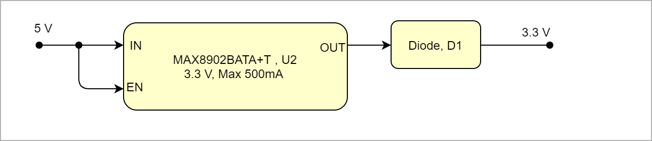 Image Modified Image Modified
|
|
Power-On Sequence
There is no specific power on sequence, after power on the Ultra96 Board all electrical components on TEP0006 will be enabled.
Power Rails
| Scroll Title |
|---|
| anchor | Table_PWR_PR |
|---|
| title | Module power rails. |
|---|
|
| Scroll Table Layout |
|---|
| orientation | portrait |
|---|
| sortDirection | ASC |
|---|
| repeatTableHeaders | default |
|---|
| style | |
|---|
| widths | |
|---|
| sortByColumn | 1 |
|---|
| sortEnabled | false |
|---|
| cellHighlighting | true |
|---|
|
| Power Rail Name | LS Expansion Connector Pin | Direction | Notes |
|---|
| +5V | 37 | Input | Supplied by Ultra96 | | VCC_PSAUX | 35 | InputOutput | Supplied by Ultra96 |
|
Technical Specifications
Absolute Maximum Ratings
| Scroll Title |
|---|
| anchor | Table_TS_AMR |
|---|
| title | PS absolute maximum ratings |
|---|
|
| Scroll Table Layout |
|---|
| orientation | portrait |
|---|
| sortDirection | ASC |
|---|
| repeatTableHeaders | default |
|---|
| style | |
|---|
| widths | |
|---|
| sortByColumn | 1 |
|---|
| sortEnabled | false |
|---|
| cellHighlighting | true |
|---|
|
| Symbols | Description | Min | Max | Unit | Vin | Input Supply Voltage | 1.7 | 5.5 | V |
|---|
| T_STG | Storage Temperature | -55 | 150 | °C |
|
...
| Scroll Title |
|---|
| anchor | Table_TS_ROC |
|---|
| title | Recommended operating conditions. |
|---|
|
| Scroll Table Layout |
|---|
| orientation | portrait |
|---|
| sortDirection | ASC |
|---|
| repeatTableHeaders | default |
|---|
| style | |
|---|
| widths | |
|---|
| sortByColumn | 1 |
|---|
| sortEnabled | false |
|---|
| cellHighlighting | true |
|---|
|
| Parameter | Min | Max | Units | Reference Document | Vin | 4.5 | 5.5 | V | See MAX8902BATA+T datasheet. |
|---|
| T_OPT | -40 | +85 | °C |
|
|
Physical Dimensions
...
| Scroll Title |
|---|
| anchor | Figure_RV_HRN |
|---|
| title | Board hardware revision number. |
|---|
|
| Scroll Ignore |
|---|
| draw.io Diagram |
|---|
| border | false |
|---|
| viewerToolbar | true |
|---|
| |
|---|
| fitWindow | false |
|---|
| diagramDisplayName | |
|---|
| lbox | true |
|---|
| revision | 34 |
|---|
| diagramName | TEP0006_RV_HRN |
|---|
| simpleViewer | false |
|---|
| width | |
|---|
| links | auto |
|---|
| tbstyle | hidden |
|---|
| diagramWidth | 188180 |
|---|
|
|
| Scroll Only |
|---|
|
|
Document Change History
...
| Scroll Title |
|---|
| anchor | Table_RH_DCH |
|---|
| title | Document change history. |
|---|
|
| Scroll Table Layout |
|---|
| orientation | portrait |
|---|
| sortDirection | ASC |
|---|
| repeatTableHeaders | default |
|---|
| style | |
|---|
| widths | |
|---|
| sortByColumn | 1 |
|---|
| sortEnabled | false |
|---|
| cellHighlighting | true |
|---|
|
| Date | Revision | Contributor | Description| |
|---|
| Page info |
|---|
| infoType | Modified date |
|---|
| dateFormat | yyyy-MM-dd |
|---|
| type | Flat |
|---|
|
| | Page info |
|---|
| infoType | Current version |
|---|
| prefix | v. |
|---|
| type | Flat |
|---|
| showVersions | false |
|---|
|
| | Page info |
|---|
| infoType | Modified by |
|---|
| type | Flat |
|---|
| showVersions | false |
|---|
|
| | -- | all | | Page info |
|---|
| infoType | Modified users |
|---|
| type | Flat |
|---|
| showVersions | false |
|---|
|
| |
|
...