...
| Page properties |
|---|
|
- Overview of Boot Mode, Reset, Enables.
|
Boot Mode must be set using DIP Switch S7 on the module TEI0022. Please note that the DIP Switch is active low.
| Scroll Title |
|---|
| anchor | Table_OV_BP |
|---|
| title | Boot process. |
|---|
|
| Scroll Table Layout |
|---|
| orientation | portrait |
|---|
| sortDirection | ASC |
|---|
| repeatTableHeaders | default |
|---|
| style | |
|---|
| widths | |
|---|
| sortByColumn | 1 |
|---|
| sortEnabled | false |
|---|
| cellHighlighting | true |
|---|
|
BOOTSEL[1..0] | DIP-switch S7 position | 00 | S7A - ON; S7B - ON| S7-1 (BOOTSEL0) | S7-2 (BOOTSEL1) | FPGA |
01S7A - ; S7B - OFF11S7A - OFF; S7B - SPI
|
| Scroll Title |
|---|
| anchor | Table_OV_RST |
|---|
| title | Reset process. |
|---|
|
| Scroll Table Layout |
|---|
| orientation | portrait |
|---|
| sortDirection | ASC |
|---|
| repeatTableHeaders | default |
|---|
| style | |
|---|
| widths | |
|---|
| sortByColumn | 1 |
|---|
| sortEnabled | false |
|---|
| cellHighlighting | true |
|---|
|
Reset | Button | Note |
|---|
HPS cold reset | S1 |
| | HPS warm reset | S3 |
| | FPGA reset | S4 |
|
|
...
| Scroll Title |
|---|
| anchor | Table_SIP_FMC |
|---|
| title | FMC connectors information |
|---|
|
| Scroll Table Layout |
|---|
| orientation | portrait |
|---|
| sortDirection | ASC |
|---|
| repeatTableHeaders | default |
|---|
| style | |
|---|
| widths | |
|---|
| sortByColumn | 1 |
|---|
| sortEnabled | false |
|---|
| cellHighlighting | true |
|---|
|
|
The FMC connector provides further interfaces like JTAG and I²C:
...
According to the JTAGEN and JTAGSEL[1..0] pins the management controller Intel MAX10 (U41), the Intel Cyclone V HPS (U10), the Intel Cyclone V FPGA (U10) or the FMC (J4) can be accessed via the micro USB B connector J13.
JTAG access is controlled by the DIP switches S7 and S8 on the module TEI0022. Please note that the DIP Switches are active low.
| Scroll Title |
|---|
| anchor | Table_SIP_JTG |
|---|
| title | JTAG pins connection |
|---|
|
| Scroll Table Layout |
|---|
| orientation | portrait |
|---|
| sortDirection | ASC |
|---|
| repeatTableHeaders | default |
|---|
| style | |
|---|
| widths | |
|---|
| sortByColumn | 1 |
|---|
| sortEnabled | false |
|---|
| cellHighlighting | true |
|---|
|
| JTAG selection | JTAG Signal State | Note | S7-3 (JTAGSEL0) | S7-4 (JTAGSEL1) | S8-4 (JTAGEN) |
|---|
JTAGSEL1 | JTAGSEL0 | JTAGSEL1 | JTAGSEL0 | Note |
|---|
| X | X | ON | Intel MAX10 |
| | ON | ON | OFF | Intel Cyclone V HPS |
| | ON | OFF | OFF | Intel Cyclone V FPGA |
| | OFF | ON | OFF | FMC |
|
|
...
| Scroll Title |
|---|
| anchor | Table_OBP |
|---|
| title | On board peripherals |
|---|
|
| Scroll Table Layout |
|---|
| orientation | portrait |
|---|
| sortDirection | ASC |
|---|
| repeatTableHeaders | default |
|---|
| style | |
|---|
| widths | |
|---|
| sortByColumn | 1 |
|---|
| sortEnabled | false |
|---|
| cellHighlighting | true |
|---|
|
|
System Controller Intel MAX 10
...
Please refer to the section "Micro USB Connector (JTAG)".
FTDI (UART)
Please refer to the section "Micro USB Connector (UART)".
DIP-Switches
There are three 4-bit DIP-switches present on the TEI0022 board to configure options and set parameters. The following section describes the functionalities of the particular switches.
...
The following figures delivers the power-on sequence information. The figure Power Sequency shows the connections between the power devices and its management. The figure Suggested Power Sequency shows the recommended firmware power-on sequence. For more information about firmware depended power-on sequencing see TEI0022 Intel MAX 10 → Power mangement.
...
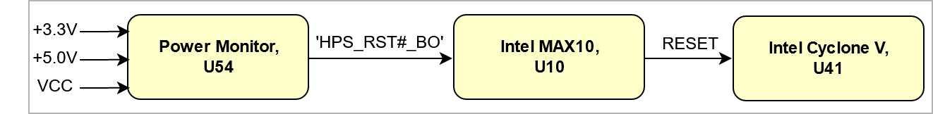
The voltages +3.3V, +5.0V, and VCC are monitored by the voltage monitor circuit LTC2911 (U54), which generates a reset signal at power-on. A manual reset is also possible as described in the reset table.
| Scroll Title |
|---|
| anchor | Figure_PWR_VMC |
|---|
| title | Voltage Monitor Circuit |
|---|
|
| Scroll Ignore |
|---|
| draw.io Diagram |
|---|
| border | true |
|---|
| viewerToolbar | true |
|---|
| |
|---|
| fitWindow | false |
|---|
| diagramDisplayName | |
|---|
| lbox | true |
|---|
| revision | 2 |
|---|
| diagramName | Figure_PWR_VMC |
|---|
| simpleViewer | true |
|---|
| width | |
|---|
| links | auto |
|---|
| tbstyle | top |
|---|
| diagramWidth | 661 |
|---|
|
|
| Scroll Only |
|---|
|
|
...