| Company | Trenz Electronic GmbH |
|---|---|
| PCN Number | PCN-20230524 |
| Title | TE0813-01 to TE0813-02 Hardware Revision Change |
| Subject | Hardware Revision Change |
| Issue Date | 2023-06-27 |
Products Affected
This change affects all Trenz Electronic TE0813 SoMs: TE0813-01*.
Affected Product | Changes | Replacement |
|---|---|---|
| TE0813-01-2AE11-A | #3...#20 | TE0813-02-2AE81-A |
| TE0813-01-2AE11-AZ | #1, #3...#20 | TE0813-02-2AE81-A |
| TE0813-01-2BE11-A | #3...#20 | TE0813-02-2BE81-A |
| TE0813-01-3AE11-A | #3...#20 | TE0813-02-3AE81-A |
| TE0813-01-3BE11-A | #3...#20 | TE0813-02-3BE81-A |
| TE0813-01-4AE11-A | #3...#20 | TE0813-02-4AE81-A |
| TE0813-01-4BE11-A | #3...#20 | TE0813-02-4BE81-A |
| TE0813-01-4BE11-AZ | #1, #3...#20 | TE0813-02-4BE81-A |
| TE0813-01-4BE81-A | #3..#20 | TE0813-02-4BE81-A |
| TE0813-01-4BE81-AZ | #1, #3...#20 | TE0813-02-4BE81-A |
| TE0813-01-4DE11-A | #3...#20 | TE0813-02-4DE81-A |
| TE0813-01-4DE11-AZ | #1, #3...#20 | TE0813-02-4DE81-A |
| TE0813-01-5DE11-A | #3...#20 | TE0813-02-5DE81-A |
| TE0813-01-5DI21-A | #2, #4...#20 | TE0813-02-5DI81-A |
Changes
#1 Changed DCDC MUN3CAD03-SE (U13, U15, U16, U19, U20, U23, U24, U29, U30, U31, U33) to TPS82085SIL and adapted voltage divider resistors.
Type: BOM Change
Reason: TPS82085SIL availability.
Impact: Minor changes in electrical characteristics.
#2 Changed DDR4 SDRAM (U2, U3, U9, U12) from K4A8G165WB-BIRC (1 GByte) to K4A8G165WC-BITDTCV (1 GByte).
Type: Schematic Change
Reason: BOM Optimization.
Impact: Memory design settings needs to be reviewed by customer.
#3 Changed DDR4 SDRAM (U2, U3, U9, U12) from NT5AD256M16D4-HR (512 MByte) to K4A8G165WC-BITDTCV (1 GByte).
Type: Schematic Change
Reason: EOL of Component.
Impact: Increased DDR4 memory size. Memory design settings needs to be reviewed by customer.
#4 Changed DCDC EN6347QI (U11) to MPM3860GQW-Z and adapted power circuit.
Type: Schematic Change
Reason: EOL of Component.
Impact: None. Increased current output capability. Minor changes in electrical characteristics.
#5 Connected DDR4-TEN signals together for U2, U3, U9, and U12 and pulled them low via 499 Ohm resistor R131. Added testpoint TP3 for signal DDR4-TEN.
Type: Schematic Change
Reason: Possible test improvement.
Impact: None.
#6 Increased voltage from 1.35 V to 1.45 V via voltage divider resistors (R33 and R38) and changed voltage rail name accordingly from PL_GT_1V35 to PL_GT_1V45.
Type: Schematic Change
Reason: Improve voltage rail behaviour.
Impact: None.
#7 Increased voltage from 1.05 V to 1.15 V via voltage divider resistors (R44 and R46) and changed voltage rail name accordingly from PL_GT_1V05 to PL_GT_1V15.
Type: Schematic Change
Reason: Improve voltage rail behaviour.
Impact: None.
#8 Added diode D2 between U41 pin 3 net MR and voltage rail 3.3VIN.
Type: Schematic Change
Reason: Protect manual reset pin.
Impact: None.
#9 Connected enable signal for DCDCs U11 and U33 from "3.3VIN" to "PG_PL_VCCINT".
Type: Schematic Change
Reason: Updated power sequence according to AMD recommendation.
Impact: None. Updated power sequence.
#10 Improved voltage rail VTT layout and added decoupling capacitors C137, C147, and C148.
Type: Schematic Change
Reason: VTT layout and decoupling improvement.
Impact: Improved VTT voltage rail reliabililty.
#11 Added DCDC (U4) VCC supply option via resistors R132 (Default: not fitted) for voltage rail PL_DCIN and R133 (Default: fitted) for voltage rail 3.3VIN.
Type: Schematic Change
Reason: Enable higher DCDC input voltage usage.
Impact: None. Option for increased input voltage usage with available backward capability.
#12 Change current limit to approximately 14.5 A for DCDC MPQ8633BGLE-Z (U4) via changing resistor R92 from 4.22 kOhm to 9.09 kOhm.
Type: Schematic Change
Reason: Fixed wrong resistor value.
Impact: None.
#13 Added option to use remote sense for DCDCs U30 via resistor R134.
Type: Schematic Change
Reason: Remote sense option.
Impact: None.
#14 Added option to use remote senses for DCDCs U29 via resistor R135.
Type: Schematic Change
Reason: Remote sense option.
Impact: None.
#15 Added option to use remote senses for DCDCs U31 via resistor R136.
Type: Schematic Change
Reason: Remote sense option.
Impact: None.
#16 Added additional decoupling capacitors C149...C157, C170...C172, C178, C187...C191, C195...C217.
Type: Schematic Change
Reason: Improve decoupling.
Impact: None.
#17 Added testpoints TP4, TP19, TP26.
Type: Schematic Change
Reason: Improve voltage measuring possibilities.
Impact: None.
#18 Added UKCA logo.
Type: PCB Change
Reason: Required for export to UK.
Impact: None.
#19 Changed 100 nF capacitors C135 and C136 from 6.3 V to 25 V.
Type: BOM Change
Reason: BOM Optimization.
Impact: None.
#20 Signal trace lengths changed
Type: PCB change
Reason: Result of changes above.
Impact: Changed trace length have to be taken into account in existing designs. The trace length for new revision will be available in TE081x series pinout generator. Please check if change in trace length still matches your requirements. Adaption of carrier may be necessary.
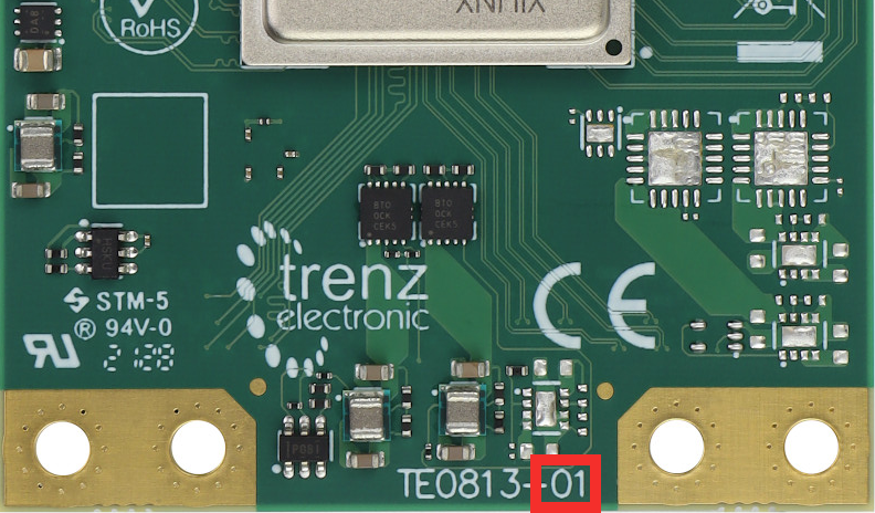
Method of Identification
The revision number is printed on the top side of the PCB.
Production Shipment Schedule
This change takes place with immediate effect. If the new revision is not suitable for your application and still the former revision of the board is needed, please contact us.
Contact Information
If you have any questions related to this PCN, please contact Trenz Electronics Technical Support at
- forum.trenz-electronic.de
- wiki.trenz-electronic.de
- support%trenz-electronic.de (subject = PCN-20230524)
phone
national calls: 05741 3200-0
international calls: 0049 5741 3200-0
Disclaimer
Any projected dates in this PCN are based on the most current product information at the time this PCN is being issued, but they may change due to unforeseen circumstances. For the latest schedule and any other information, please contact your local Trenz Electronic sales office, technical support or local distributor.
This PCN follows JEDEC Standard J-STD-046.
Overview
Content Tools