| Company | Trenz Electronic GmbH |
|---|---|
| PCN Number | PCN-20200615 |
| Title | TE0835-01 to TE0835-02 Hardware Revision Change |
| Subject | Hardware Revision Change |
| Issue Date | 2020-07-02 |
This change affects all Trenz Electronic TE0835 SoMs of revision 01: TE0835-01-*.
Affected Product | Replacement |
|---|---|
| TE0835-01-* | TE0835-02-* |
Type: Schematic change
Reason: Some I/O standards with DCI need external VRP.
Impact: DCI I/O standarts with external VRP usable on this bank.
Type: Schematic change
Reason: Primilary installed LDO had disadvantegous output discarge function, which prevents external sourcing of 3.3V_CPLD rail.
Impact: External sourcing of 3.3V_CPLD rail possible.
Type: Schematic change
Reason: Improve routing/signal integrity.
Impact: Signal DBG_LED3 is connected on AD18 pin of FPGA, was AE18.
Type: Schematic change
Reason: Improve routing/signal integrity.
Impact: Signal FPGA_IO0 to CPLD now available at Pin AE18, was AF17.
Type: Schematic change
Reason: PS periphery controller with fixed IO assignments may need MIO13 (e.g. for eMMC).
Impact: MIO13 now availabe at B2B J1, if still MIO25 is needed a jumper resistor has to moved from R76 to R84.
Type: Schematic change
Reason: MIO13 is now user IO.
Impact: No pullup on MIO13.
Type: PCB change
Reason: MIO13 is now user IO.
Impact: It is no more possible to control LED D1 via MIO13.
Type: Schematic change
Reason: Improve solution for enabling CPLD JTAG.
Impact: CPLD update possible when JTAG enabled via shortcut of THT testpoints, also installation of pinheader with jumper possible.
Type: Schematic change
Reason: Inconsistent net naming.
Impact: Nets named according to resident Bank.
Type: BOM change
Reason: Compensation of U7 did not work.
Impact: U7 stable working.
Type: PCB change
Reason: Lenght matching required.
Impact: Clks correctly length matched.
Type: PCB change
Reason: BIAS routed to wrong Powerrail.
Impact: U8 working correctly.
Type: Schematic change
Reason: PGOOD did not work.
Impact: PGOOD of U7 works correct.
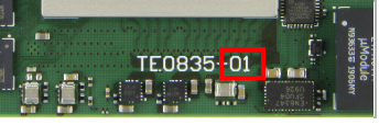
The revision number is printed on the top side of the PCB.
The new revison 02 is available from August 2020.
If you have any questions related to this PCN, please contact Trenz Electronics Technical Support at
phone
national calls: 05741 3200-0
international calls: 0049 5741 3200-0
Any projected dates in this PCN are based on the most current product information at the time this PCN is being issued, but they may change due to unforeseen circumstances. For the latest schedule and any other information, please contact your local Trenz Electronic sales office, technical support or local distributor.
This PCN follows JEDEC Standard J-STD-046.