Template Revision 1.9 - on construction Design Name always "TE Series Name" + optional CPLD Name + "CPLD" |
<!-- tables have all same width (web max 1200px and pdf full page(640px), flexible width or fix width on menu for single column can be used as before) -->
<style>
.wrapped{
  width: 100% !important;
  max-width: 1200px !important;
 }
</style> |
Table of contents |
Firmware for RFSoC module CPLD with designator U31: LCMX02-640HC
See Document Change History
| Name / opt. VHD Name | Direction | Pin | Bank Power | Description |
|---|---|---|---|---|
| PWR_STATUS | out | 36 | 1.8V_CPLD | Output for Status-LED (After successful configuration of FPGA is connected automatically with FPGA_IO0) |
| MODE0 | out | 35 | 1.8V_CPLD | ZynqMP boot mode pin 0 |
| PG_VCCRF | in | 34 | 1.8V_CPLD | Power Good input from PWR_PRE |
| SRST_B | out | 33 | 1.8V_CPLD | FPGA external system reset / currently_not_used |
| PROG_B | out | 32 | 1.8V_CPLD | FPGA reset PL configuration logic / currently_not_used |
| PG_GR2 | in | 31 | 1.8V_CPLD | Power control input from PWR_PS and PWR_DDR |
| MIO28_UART1_TX | out | 29 | 1.8V_CPLD | UART Transmition pin / currently_not_used |
| MIO28_UART1_RX | in | 28 | 1.8V_CPLD | UART Receive pin / currently_not_used |
| FPGA_IO0 | out | 27 | 1.8V_CPLD | FPGA GPIO / User LED |
| FPGA_IO1 | inout | 26 | 1.8V_CPLD | FPGA GPIO / User dip switch interface |
| EN_PS_PL | out | 14 | 3.3V_CPLD | Power enable for PWR_CORE , PWR_PS and PWR_GT |
| EN_GR1 | out | 15 | 3.3V_CPLD | Power enable for PWR_GT and PWR_PS |
| EN_RF_ADC | out | 16 | 3.3V_CPLD | Power enable for PWR_ADC |
| PG_RF_DAC | in | 17 | 3.3V_CPLD | Power control input from PWR_DAC |
| EN_VCCRF | out | 18 | 3.3V_CPLD | Power enable for PWR_PRE |
| EN_GR2 | out | 19 | 3.3V_CPLD | Power enable for PWR_DDR , PWR_GT and PWR_PS |
| PG_PS_PL | in | 20 | 3.3V_CPLD | power control input from PWR_CORE , PWR_GT and PWR_PS |
| PG_GR1 | in | 21 | 3.3V_CPLD | Power control input from PWR_GT and PWR_PS |
| PG_RF_ADC | in | 23 | 3.3V_CPLD | Power control input from PWR_ADC |
| EN_RF_DAC | out | 24 | 3.3V_CPLD | Power enable for PWR_DAC |
| MODE2 | out | 2 | 1.8V_CPLD | ZynqMP boot mode pin 2 |
| MODE1 | out | 3 | 1.8V_CPLD | ZynqMP boot mode pin 1 |
| POR_B | out | 4 | 1.8V_CPLD | Power-On reset signal |
| MODE3 | out | 5 | 1.8V_CPLD | ZynqMP boot mode pin 3 |
| INIT_B | in | 7 | 1.8V_CPLD | FPGA PL initialization activity and configuration error signal / currently_not_used |
| F_TDI | out | 8 | 1.8V_CPLD | JTAG ZynqMP |
| F_TMS | out | 9 | 1.8V_CPLD | JTAG ZynqMP |
| F_TCK | out | 10 | 1.8V_CPLD | JTAG ZynqMP |
| F_TDO | in | 11 | 1.8V_CPLD | JTAG ZynqMP |
| DONE | in | 12 | 1.8V_CPLD | FPGA PL configuration done indicator |
| JTAG_TDO | out | 48 | 3.3V_CPLD | JTAG_B2B |
| JTAG_TDI | in | 47 | 3.3V_CPLD | JTAG_B2B |
| JTAG_TCK | in | 45 | 3.3V_CPLD | JTAG_B2B |
| JTAG_TMS | in | 44 | 3.3V_CPLD | JTAG_B2B |
| CPLD_IO0 | in | 43 | 3.3V_CPLD | BOOT Mode input pin 0 |
| CPLD_IO1 | in | 42 | 3.3V_CPLD | BOOT Mode input pin 1 |
| CPLD_JTAGEN | in | 41 | 3.3V_CPLD | Enable JTAG access to CPLD for Firmware update (zero: JTAG routed to module, one: CPLD access) |
| CPLD_IO2 | in | 40 | 3.3V_CPLD | CPLD IO to B2B / Used as dip switch interface on the carrier board (After successful configuration of FPGA is connected automatically with FPGA_IO1) |
| CPLD_IO3 | out | 38 | 3.3V_CPLD | CPLD IO to B2B/ Used as power good, can be used to enable carrier periphery power |
| RESETN | in | 37 | 3.3V_CPLD | Reset pin (Active low) |
JTAG signals routed directly through the CPLD to FPGA. Access between CPLD and FPGA can be multiplexed via JTAGEN (logical one for CPLD, logical zero for FPGA) on B2B. In the carrier board TEB0835 can be activated this pin with S1-4 dip switch.
| CPLD_JTAGEN (B2B J1-30) | S1-4 on TEB0835 Carrier Board | Description |
|---|---|---|
| 0 | OFF | FPGA access |
| 1 | ON | CPLD access |
In this module the CPLD is responsible for controlling the power of the module. There are different power regulators or DC/DC converters whose outputs can be controlled by an enable signal. At the same time the outputs can also be monitored by power-good signals.
| Enable Signal | Power Good Signal | Schematic page | Net | Domain | Regulator/ DC-DC Converter | in/out Voltage |
|---|---|---|---|---|---|---|
| EN_PS_PL | PG_PS_PL | PWR_CORE PWR_PS PWR_GT | VCCINT, VCINT_IO, VCCBRAM PSINTLP/PSINTFP,PSINTFP_DDR MGTAVCC | PL PS_LP/PS_FP GTH | LTM4662EY LTM4644EY TPS82085 | 5V/0.835V 5V/0.85V 5V/0.9V |
| EN_GR1 | PG_GR1 | PWR_PS PWR_GT PWR_GT | PSAUX,PSADC,PSIO/VCCAUX,VCCAUX_IO/PS_DDR_PLL PSMGTRAVCC/MGTVCCAUX PSPLL/MGTAVTT | PS_LP/PL/PS_FP PS_FP/GTH PS_LP/GTH | TPS82085 EP53A7LQI EN6347QI | 5V/1.8V 5V/0.85V 5V/1.2V |
| EN_GR2 | PG_GR2 | PWR_PS PWR_GT PWR_DDR PWR_DDR | VCC_B88_HD PS_MGTRAVTT DDR_2V5 DDR_1V2 | PS_LP PS_FP DDR DDR | TPS82085 EP53A7HQI TPS82085 TPS82085 | 5V/3.3V 5V/1.8V 5V/2.5V 5V/1.2V |
| EN_VCCRF | PG_VCCRF | PWR_PRE | VCCINT_AMS, APRE_1V15, APRE_3V3 | ADC and DAC | LTM4644EY | 5V/0.8534V,1.15V,3.3V |
| EN_RF_ADC | PG_RF_ADC | PWR_ADC PWR_ADC | ADC_AVCC ADC_AVCCAUX | ADC ADC | TPS74401 TPS74401 | 1.15V/0.925V 3.3V/1.8V |
| EN_RF_DAC | PG_RF_DAC | PWR_DAC PWR_DAC PWR_DAC | DAC_AVCC DAC_AVCCAUX DAC_AVTT | DAC DAC DAC | TPS74801 TPS74801 TPS74801 | 5V/0.925V 5V/1.8V 5V/2.5V |
According to the Xilinx instructions the power regulator or DC-DC converter must be switched on or off in a certain order. This is called power-on or power-off sequencing.To implement power-on sequencing correctly, a state machine must be running there. In the following you can see the State Machine Diagram.
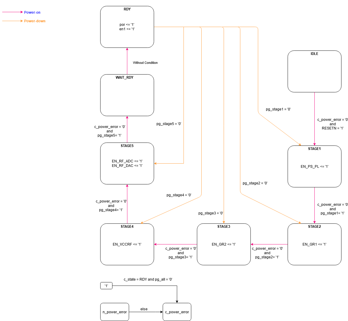
| Stage | Control | Voltage Domains | Signal Monitoring to change stage |
|---|---|---|---|
| IDLE | --- | --- | RESETN |
| STAGE1 | EN_PS_PL enabled (High) | 0.853V, 0.85V, 0.9V | PG_PS_PL |
| STAGE2 | EN_GR1 enabled (High) | 1.8V, 0.85V, 1.2V | PG_GR1 |
| STAGE3 | EN_GR2 enabled (High) | 3.3V, 1.8V | PG_GR2 |
| STAGE4 | EN_VCCRF enabled (High) | 0.8534V, 1.158V, 3.3V | PG_VCCRF |
| STAGE5 | EN_RF_ADC enabled (High) EN_RF_DAC enabled (High) | 0.925V, 1.8V 0.925V, 1.8V, 2.5V | PG_RF_ADC PG_RF_DAC |
| WAIT_RDY | --- | --- | --- |
| RDY | por enabled (High) en1 enabled (High) if DONE is High. | --- | pg_all |
| States | Blink Sequence | Comment |
|---|---|---|
| IDLE | ooooooooooooooooooo* | Power Sequencing can not start. RESETN is active. |
| Stage 1 | ooooooooooooooooo*o* | The correct voltage in one of the following nets are failed: VCCINT, VCINT_IO, VCCBRAM, PSINTLP, PSINTFP, PSINTFP_DDR, MGTAVCC |
| Stage 2 | ooooooooooooooo*o*o* | The correct voltage in one of the following nets are failed: PSAUX, PSADC, PSIO, VCCAUX, VCCAUX_IO, PS_DDR_PLL, PSMGTRAVCC, MGTVCCAUX, PSPLL, MGTAVTT |
| Stage 3 | ooooooooooooo*o*o*o* | The correct voltage in one of the following nets are failed: VCC_B88_HD, PS_MGTRAVTT, DDR_2V5 , DDR_1V2 |
| Stage 4 | ooooooooooo*o*o*o*o* | The correct voltage in one of the following nets are failed: VCCINT_AMS, APRE_1V15, APRE_3V3 |
| Stage 5 | ooooooooo*o*o*o*o*o* | The correct voltage in one of the following nets are failed: ADC_AVCC, ADC_AVCCAUX, DAC_AVCC, DAC_AVCCAUX, DAC_AVTT |
| WAIT_RDY / RDY and DONE='0' | ooooooo*o*o*o*o*o*o* | Power is ok. But the FPGA is not yet configured. |
| pg_all = '0' | ooooo*o*o*o*o*o*o*o* | An unknown error has occurred. The power supply must be switched off. |
| USR (RDY and DONE='1') | User defined | Power is ok and the FPGA is configured successfully. LED can be controlled by user, when Power is OK and FPGA part is programmed (DONE signal is high) |
If the FPGA correctly programmed (DONE signal is high) and the power-on sequencing state is RDY then the User IOs can be shown in the following table:
| Function | Interface | Schematic | FPGA Pin | Note |
|---|---|---|---|---|
| USER signal | B2B (J1-32) | FPGA_IO1 | AE16 | source by TEB0835 Dip Switch S1-3, in case FPGA is programmed |
| LED (D1) | -- | FPGA_IO0 | AE18 | controls LED, in case FPGA is programmed |
Boot Modes can be selected via B2B Pin Mode.
| B2B Pin J1-28 (CPLD IO1) | B2B Pin J1-26 (CPLD IO0) | Boot Mode |
|---|---|---|
| 0 | 0 | Boot from PS JTAG |
| 0 | 1 | Boot from QSPI |
| 1 | 1 | Boot from SD Card |
To get content of older revision got to "Change History" of this page and select older document revision number.
|
| Date | Document Revision | CPLD Firmware Revision | Supported PCB Revision | Authors | Description |
|---|---|---|---|---|---|
| REV01 | REV02, REV01 |
| |||
| 2020-08-18 | v.4 | REV00 | REV01 | Ivan Girshchenko / Mohsen Chamanbaz |
|
| All |