Template Revision 2.12
- Module: TRM Name always "TE Series Name" +TRM
Example: "TE0728 TRM" - Carrier: TRM Name usually "TEB Series Name" +TRM
Example: "TEB0728 TRM"
|
<!-- tables have all same width (web max 1200px and pdf full page(640px), flexible width or fix width on menu for single column can be used as before) -->
<style>
.wrapped{
  width: 100% !important;
  max-width: 1200px !important;
 }
</style> |
----------------------------------------------------------------------- |
Note for Download Link of the Scroll ignore macro: |
Table of Contents 
|
Overview
The Trenz Electronic TEM0005-02 is a low-cost module with Microsemi SmartFusion2 SoC and 32 MByte flash memory for configuration and operation. SmartFusion2 combines a 166 MHz Cortex-M3 MCU with 256 KByte Flash and 80 KByte SRAM as well as 12 kLUT FPGA Core Logic.
Refer to http://trenz.org/tem0005-info for the current online version of this manual and other available documentation.
Key Features
Note:
'description: Important components and connector or other Features of the module
→ please sort and indicate assembly options Key Features' must be split into 6 main groups for modules and mainboards: - SoC/FPGA
- Package: SFVC784
- Device: ZU2...ZU5*
- Engine: CG, EG, EV*
- Speed: -1LI, -2LE,*, **
- Temperature: I, E,*, **
- RAM/Storage
- Low Power DDR4 on PS
- Data width: 32bit
- Size: def. 2GB*
- Speed:***
- eMMC
- Data width: 8Bit
- size: def. 8GB *
- QSPI boot Flash in dual parallel mode (size depends on assembly version)
- Data width: 8bit
- size: def. 128MB *
- HyperRAM/Flash (optional, default not assembled)
- MAC address serial EEPROM with EUI-48™ node identity (Microchip 24AA025E48)
- On Board
- Lattice LCMXO2
- PLL SI5338
- Gigabit Ethernet transceiver PHY (Marvell Alaska 88E1512)
- Hi-speed USB2 ULPI transceiver with full OTG support (Microchip USB3320C)
- Interface
- 132 x HP PL I/Os (3 banks)
- ETH
- USB
- 4 GTR (for USB3, Sata, PCIe, DP)
- MIO for UART
- MIO for SD
- MIO for PJTAG
- JTAG
- Ctrl
- Power
- 3.3V-5V Main Input
- 3.3V Controller Input
- Variable Bank IO Power Input
- Dimension
- Notes
- * depends on assembly version
- ** also non low power assembly options possible
- *** depends on used U+ Zynq and DDR4 combination
Key Features' must be split into 6 main groups for carrier: - Modules
- TE0808, TE807, TE0803,...
- RAM/Storage
- On Board
- Interface
- E.g. ETH, USB, B2B, Display port
- Power
- E.g. Input supply voltage
- Dimension
|
- SoC/FPGA
- Package: VFG400
- Device: M2S010, M2S050 *
- Engine: 166Mhz 32Bit ARM Cortex-M3
- Speed: Standard
- Temperature: C, I*
- RAM/Storage
- Low Power DDR3
- Data width: 16bit
- Size: def. 2Gb
- SPI Flash
- 2Kb EEPROM
- On Board
- Crypto Authentication IC
- Voltage monitor IC
- 10/100 Mbps PHY Ethernet
- Interface
- Power
- 3.3V supplied from carrier
- Dimension
- Notes
- * depends on assembly version
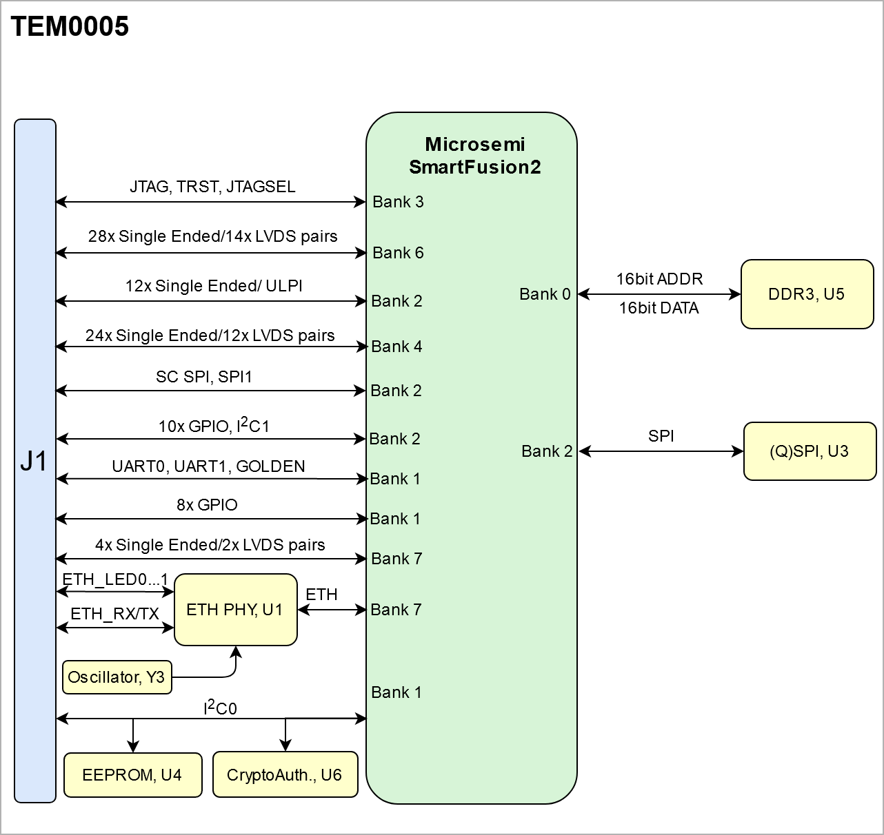
Block Diagram
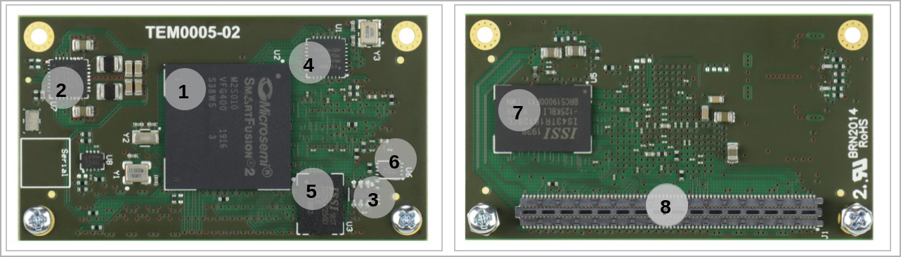
Main Components
Notes : - Picture of the PCB (top and bottom side) with labels of important components
- Add List below
|
- Microsemi SmartFusion2 SoC, U2
- Dual DCDC Regulator, U7
- EEPROM, U4
- 10/100 Mb Ethernet, U1
- QSPI Flash, U3
- Authentication IC, U6
- DDR3 Memory, U5
- B2B Connector, J1
Initial Delivery State
Notes : Only components like EEPROM, QSPI flash can be initialized by default at manufacture. If there is no components which might have initial data ( possible on carrier) you must keep the table empty |

Storage device name | Content | Notes |
|---|
Quad SPI Flash | Not Programmed |
| | EEPROM | Not Programmed |
| | CryptoAuthentication | Not Programmed |
|
|
Configuration Signals
- Overview of Boot Mode, Reset, Enables.
|
Signal | B2B | I/O | Note |
|---|
RESET
| J1-11 |
| Active low reset |
|
Signals, Interfaces and Pins
Notes : - For carrier or stand-alone boards use subsection for every connector type (add designator on description, not on the subsection title), for example:
- For modules which needs carrier use only classes and refer to B2B connector if more than one is used, for example
|
Board to Board (B2B) I/Os
FPGA bank number and number of I/O signals connected to the B2B connector, J1.
| FPGA Bank | Interface | I/O Signal Count | Voltage Level | Notes |
|---|
| Bank 1 | GPIO | 8x Single Ended | 3.3V |
| | UART | 4x Single Ended | 3.3V |
| | I2C | 2x Single Ended | 3.3V |
| | GOLDEN | 1x Single Ended | 3.3V |
| | Bank 2 | ULPI/I/O | 12x Single Ended | 3.3V |
| | I2C | 2x Single Ended | 3.3V |
| | GPIO | 10x Single Ended | 3.3V |
| | SC SPI | 4x Single Ended | 3.3V |
| | SPI1 | 7x Single Ended | 3.3V |
| | Bank 3 | JTAG | 5x Single Ended | 3.3V |
| | Reset | 1x Single Ended | 3.3V |
| | Bank 4 | I/O | 24x Single Ended/12 LVDS pairs | 3.3V |
| | Bank 6 | I/O | 28x Single Ended/14 LVDS pairs | VDDI6 | max 2.5V | | Bank 7 | I/O | 4x Single Ended | 3.3V |
|
|
JTAG Interface
JTAG access to the TEM0005 SoM through B2B connector J1.
JTAG Signal | B2B Connector |
|---|
| TMS | J1-14 | | TDI | J1-8 | | TDO | J1-10 | | TCK | J1-12 | | TRST | J1-7 |
|
Test Points
you must fill the table below with group of Test Point which are indicated as TP in a schematic. If there is no Test Point remarked in the schematic, delet the Test Point section. Example: | Test Point | Signal | B2B | Notes |
|---|
| 10 | PWR_PL_OK | J2-120 |
|
|
| Test Point | Signal | Connected to | Notes |
|---|
| TP1 | CLKOUT | Regulator, U7 |
|
|
On-board Peripherals
Notes : - add subsection for every component which is important for design, for example:
- Two 100 Mbit Ethernet Transciever PHY
- USB PHY
- Programmable Clock Generator
- Oscillators
- eMMCs
- RTC
- FTDI
- ...
- DIP-Switches
- Buttons
- LEDs
|
Notes : In the on-board peripheral table "chip/Interface" must be linked to the corresponding chapter or subsection |
(Quad) SPI Flash Memory
Notes : Minimum and Maximum density of quad SPI flash must be mentioned for other assembly options. |
The TEM0005 is equipped with a (Q)SPI flash memory, U3 provided in order to store data and configuration.
| Schematic | U3 Pin | Connected to | Notes |
|---|
| SPI0_SS0 | nCE | FPGA Bank 2 |
| | SPI0_CLK | SCK | FPGA Bank 2 |
| | SPI0_SDO | SI/IO0 | FPGA Bank 2 |
| | SPI0_SDI | SO/IO0 | FPGA Bank 2 |
|
|
EEPROM
The TEM0005 is equipped with an EEPROM IC, U4. The I2C signals are connected to authentication IC as well.
| Schematic | U4 Pin | Notes |
|---|
| I2C0_SCL | SCL |
| | I2C0_SDA | SDA |
|
|
| Pin | I2C Address | Designator | Notes |
|---|
| SCL/SDA | 0x70 | U4 |
|
|
Authentication IC
There is an Authentication IC ATECC608A provided on TEM0005, The IC is connected to I2C0 bus.
| Pin | Schematic | Notes |
|---|
| SCL | I2C0_SCL | Serial Clock | | SDA | I2C1_SCL | Serial Data |
|
| Pin | I2C Address | Designator | Notes |
|---|
| SCL/SDA | 0xC0 | U6 | This is the default value, which can be changed, see device datasheet. |
|
DDR3L SDRAM
Notes : Minimum and Maximum density of DDR3 SDRAM must be mentioned for other assembly options. (pay attention to supported address length for DDR3) |
The TEM0005 SoM has 2 Gb volatile DDR3L SDRAM IC for storing user application code and data.
- Part number: IS43TR16128CL-125KBLI
- Supply voltage: 1.5 V
- Temperature: -40 to 95 °C
Ethernet Transceiver
On board 10/100 Mbps Ethernet Transceiver U1 is provided on the module TEM0005.
| U1 Pin | Signal Name | Connected to | Note |
|---|
| RXM/RXP | ETH1_RX | B2B, J1 |
| | TXM/TXP | ETH1_TX | B2B, J1 |
| | LED0/NWAYEN | ETH1_LED0 | B2B, J1 |
| | LED1/SPEED | ETH1_LED1 | B2B, J1 |
| | MDIO | ETH1_MDIO | FPGA Bank 7, U2 |
| | MDC | ETH1_MDC | FPGA Bank 7, U2 |
| | REXT | - | GND |
| | INTRP | ETH1_INTRP | FPGA Bank 7, U2 |
| | XO/XI | - | Crystal Oscillator, Y3 |
| | nRST | ETH1_RST | FPGA Bank 7, U2 |
| | CONFIG0...2 | ETH1_COL/CRC/RXDV | FPGA Bank 7, U2 |
| | TXC | ETH1_TXC | FPGA Bank 7, U2 |
| | TXEN | ETH1_TXEN | FPGA Bank 7, U2 |
| | TXD0...3 | ETH1_TXD0...3 | FPGA Bank 7, U2 |
| | RXD0...3 | ETH1_RXD0...3 | FPGA Bank 7, U2 |
| | RXC | ETH1_RXC | FPGA Bank 7, U2 |
| | RXCER | ETH1_RXCER | FPGA Bank 7, U2 |
|
|
Clock Sources
| Designator | Description | Frequency | Note |
|---|
| Y3 | Crystal Oscillator | 25 MHz | Connected to ETH PHY |
|
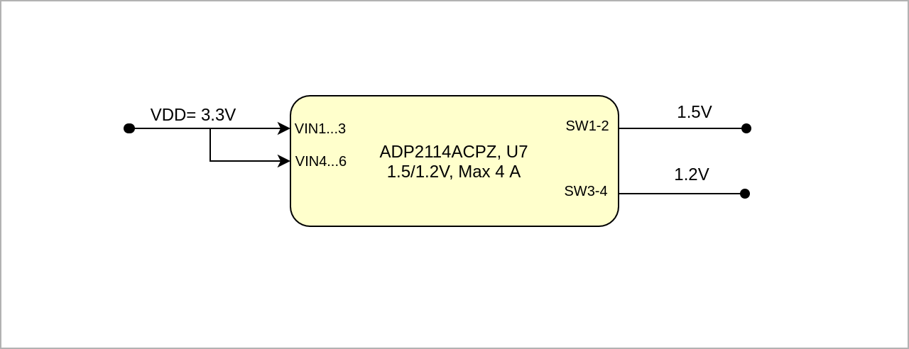
Power and Power-On Sequence
In 'Power and Power-on Sequence' section there are three important digrams which must be drawn: - Power on-sequence
- Power distribution
- Voltage monitoring circuit
|
Power Supply
Power supply with minimum current capability of 1.5 A for system startup is recommended.
Power Consumption
| Power Input Pin | Typical Current |
|---|
| VIN | TBD* |
|
* TBD - To Be Determined
Power Distribution Dependencies
Power-On Sequence
Voltage Monitor Circuit
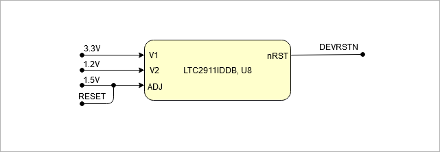
The TEM0005 is equipped with a voltage monitoring IC, U8. Reset Logic Output (nRST) asserts low when any of the V1, V2, or ADJ inputs are below their reset thresholds.
Power Rails
| Power Rail Name | B2B Connector J1 Pin | Direction | Notes |
|---|
| 3.3V | 1, 2, 3, 4 | Input |
| | VDDI6 | 22 | Input |
|
|
Bank Voltages
| Schematic Name | | Notes |
|---|
| Bank0 | 1.5V | 1.5V |
| | Bank1 | 3.3V | 3.3V |
| | Bank2 | 3.3V | 3.3V |
| | Bank3 | 3.3V | 3.3V |
| | Bank4 | 3.3V | 3.3V |
| | Bank5 | 3.3V | 3.3V |
| | Bank6 | VDDI6 | max. 2.5V | supplied by carrier | | Bank7 | 3.3V | 3.3V |
|
|
Board to Board Connectors
- This section is optional and only for modules.
use "include page" macro and link to the general B2B connector page of the module series, For example: 6 x 6 SoM LSHM B2B Connectors

|

Technical Specifications
Absolute Maximum Ratings
| Symbols | Description | Min | Max | Unit |
|---|
| VIN | Input Supply Voltage | -0.3 | 3.63 | V | | STG_T | Storage Temperature | -45 | 125 | °C |
|
Recommended Operating Conditions
Operating temperature range depends also on customer design and cooling solution. Please contact us for options.
| Parameter | Min | Max | Units | Reference Document |
|---|
| VIN | 3.15 | 3.45 | V | See the carrier datasheets. | | OPT_T | 0 /-40 | 85 | °C | See Microsemi Smartfusion2 datasheet. Depends on assembly version. |
|
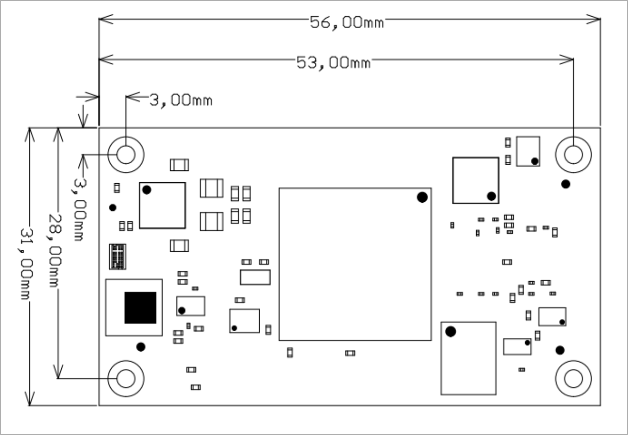
Physical Dimensions
PCB thickness: 1.6 mm.
Currently Offered Variants
Revision History
Hardware Revision History
| Date | Revision | Changes | Documentation Link |
|---|
| 2019-10-01 | REV01 | | REV01 | | 2020-05-20 | REV02 | - Support M2S050 ->added R29,R30, C24..C26,C31
- Added resistor R32
- Full upd LIB
| REV02 |
|
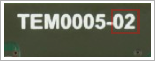
Hardware revision number can be found on the PCB board together with the module model number separated by the dash.
Document Change History
- Note this list must be only updated, if the document is online on public doc!
- It's semi automatically, so do following
Add new row below first Copy "Page Information Macro(date)" Macro-Preview, Metadata Version number, Author Name and description to the empty row. Important Revision number must be the same as the Wiki document revision number Update Metadata = "Page Information Macro (current-version)" Preview+1 and add Author and change description. --> this point is will be deleted on newer pdf export template - Metadata is only used of compatibility of older exports
|
| Date | Revision | Contributor | Description |
|---|
| | 
| | -- | all | 
| |
|
Disclaimer