Template Revision 2.9 - on construction Design Name always "TE Series Name" + optional CPLD Name + "CPLD"
|
Overview
Lattice MachXO2-4000HC is a CPLD chip, that is used in TEB0912 board as a system management controller. The system controller implements power management same as power sequencing, . Rather than power management is the system controller responsible for reset generation, zynq initial configuration. System controller contains of some additional features same as debouncing the power button and displaying the power status with LEDs. The JTAG and UART interfaces are routed in the firmware of CPLD from FTDI chip to FPGA. In this board the CPLD is responsible for controlling and monitoring of power supply of the board. There are various DC-DC converter or regulators , one input current sensor and six temperature sensors. To control every converter chip or regualtor monitors CPLD power good outputs of regulators or DC-DC converters continuously to avoid over-voltage in the power system. System controller reads the measured temperature of all temperature sonsors continuously to avoid over-temperature in regulators or DC-DC converter chips. The firmware of CPLD contains of various subsystems same as i2c master and i2c slave subsystems. I2c master reads the data of current sensor and 6 temperature sensors , that measure the temperature of DC-DC converter chips. I2c slave is responsible for communicating with FPGA to read register addresses and write the measured data in FPGA.
Feature Summary
- Power Management
- Reset Management
- JTAG Routing
- Boot Mode
- User IOs
- LED and power state display
- UART
- I2C Slave
- I2C Master
- I2C to GPIO
- RAM Memory
- Data Management State Machine
- Temperature Sensor TMP461
- Current Sensor INA219AIDCNR
Firmware Revision and supported PCB Revision
See Document Change History
Product Specification
Port Description
| Name / opt. VHDL Name | Direction | Pin | Pullup/Down (HW) | Bank Power | Description |
|---|---|---|---|---|---|
| ALERT_N | in | B33 | --- (UP) | +3.3V_STB | Digital output . Interrupt or SMBus alert output of temperature sensors (TMP461AIRUNT- U43,U47,U52,U57,U4) and temperature sensor with integrated fan control (LM96163-U61) /currently_not_used |
| CPLD_DEBUG0 | inout | A41 | NONE (UP) | +3.3V_STB | CPLD debug pin 0 |
| CPLD_DEBUG1 | inout | A2 | UP (UP) | +3.3V_STB | CPLD debug pin 1 --→ For monitoring of I2C master clock (SCL) |
| CPLD_DEBUG2 | inout | B1 | UP (UP) | +3.3V_STB | CPLD debug pin 2 --→ For monitoring of I2C master data (SDA) |
| CPLD_DEBUG3 | inout | A3 | --- (NONE) | +3.3V_STB | CPLD debug pin 3 /currently_not_used |
| CPLD_HD0 | inout | B3 | UP (UP) | +3.3V_STB | High density IOs select 0 |
| CPLD_HD1 | inout | B28 | UP (UP) | +3.3V_STB | High density IOs select 1 |
| EN_VCCINT | out | B22 | NONE (DOWN) | +3.3V_STB | Enable pin for +0.85V DC-DC converter (LTM4630EY-U42A) |
| EN_VTT_DDR | out | A22 | NONE (DOWN) | +3.3V_STB | Enable pin for 2A Peak Sink/Source DDR Termination Regulator (TPS51206-U2, U3) |
| EN+0.85V_GT_AVCC_PS/ EN_0V85_GT_AVCC_PS | out | B21 | NONE (DOWN) | +3.3V_STB | Enable pin for 1.5A low-dropout linear regulator (TPS74801DRC-U45) |
| EN+0.9V_GT_AVCC/ EN_0V9_GT_AVCC | out | B14 | NONE (DOWN) | +3.3V_STB | Enable pin for quad DC-DC microModule regulator with configurable 4A output array for +0.9V output voltage (LTM4644EY-U44) |
| EN+1.0V/ EN_1V0 | out | A46 | NONE (DOWN) | +3.3V_STB | Enable pin for 1.5A low-dropout linear regulator with +1.0V output voltage (TPS74801DRC-U13) |
| EN+1.2V_DDR/ EN_1V2_DDR | out | A34 | NONE (DOWN) | +3.3V_STB | Enable pin for quad DC-DC microModule regulator with configurable 4A output array for +1.2V output voltage (LTM4644EY-U53) |
| EN+1.2V_GT_AVTT/ EN_1V2_GT_AVTT | out | B16 | NONE (DOWN) | +3.3V_STB | Enable pin for quad DC-DC microModule regulator with configurable 4A output array for +1.2V output voltage (LTM4644EY-U48) |
| EN+1.2V_PLL_PS/ EN_1V2_PLL_PS | out | A15 | NONE (DOWN) | +3.3V_STB | Enable pin for 1.5A low-dropout linear regulator (TPS74801DRC-U46) |
EN+1.3V_MGT_PS/ | out | B15 | NONE (DOWN) | +3.3V_STB | Enable pin for quad DC-DC microModule regulator with configurable 4A output array for +1.37V output voltage (LTM4644EY-U44) |
| EN+1.8V/ EN_1V8 | out | B13 | NONE (DOWN) | +3.3V_STB | Enable pin for quad DC-DC microModule regulator with configurable 4A output array for +1.8V output voltage (LTM4644EY-U53) |
| EN+1.8V_AUX/ EN_1V8_AUX | out | A30 | NONE (DOWN) | +3.3V_STB | Enable pin for 1.5A low-dropout linear regulator with +1.8V output voltage (TPS74801DRC-U49,U50,U51) |
| EN+1.8V_GT_AVTT_PS/ EN_1V8_GT_AVTT_PS | out | B20 | NONE (DOWN) | +3.3V_STB | Enable pin for 1.5A low-dropout linear regulator with +1.8V output voltage (TPS74801DRC-U54) |
| EN+2.5V_DDR/ EN_2V5_DDR | out | A44 | NONE (DOWN) | +3.3V_STB | Enable pin for 1.5A low-dropout linear regulator with +2.5V output voltage (TPS74801DRC-U55, U56) |
| EN+2V_MGT_PS/ EN_2V0_GT_PS | out | A21 | NONE (DOWN) | +3.3V_STB | Enable pin for quad DC-DC microModule regulator with configurable 4A output array for +2.0V output voltage (LTM4644EY-U48) |
| EN+3.3V/ EN_3V3 | out | B18 | NONE (DOWN) | +3.3V_STB | Enable pin for quad DC-DC microModule regulator with configurable 4A output array for +3.3V output voltage (LTM4644EY-U1) |
| EN+5V_BIAS/ EN_5V_VBIAS | out | A17 | NONE (DOWN) | +3.3V_STB | Enable pin for low dropout linear regulator with +5V output voltage (ADP7102ACPZ-U58) |
| EXT_STATUS_LED_G | out | B9 | --- (NONE) | +3.3V_STB | External status LED green (J40-Pin2) /currently_not_used |
| EXT_STATUS_LED_R | out | A25 | --- (NONE) | +3.3V_STB | External status LED red (J40-Pin3) /currently_not_used |
| FAN_EN | out | B29 | NONE (UP) | +3.3V_STB | Enables a smart high-side power switch to drive the FAN (BTS41411N-U60) |
| FPGA_DONE | in | A24 | NONE (UP) | +3.3V_STB | FPGA PL configuration done indicator |
| FTDI_PWR_EN_N | in | A36 | NONE (UP) | +3.3V_STB | Active low power enable output of FTDI chip (FT2232H56Q-U38) |
| FTDI_RX | out | A35 | NONE (NONE) | +3.3V_STB | UART RXD of FTDI chip (FT2232H56Q-U38) |
| FTDI_TCK | in | A45 | UP (NONE) | +3.3V_STB | FTDI JTAG clock pin (FT2232H56Q-U38) |
| FTDI_TDI | in | A47 | UP (NONE) | +3.3V_STB | FTDI JTAG data input pin (FT2232H56Q-U38) |
| FTDI_TDO | out | A48 | NONE (NONE) | +3.3V_STB | FTDI JTAG data output pin (FT2232H56Q-U38) |
| FTDI_TMS | in | B34 | NONE (NONE) | +3.3V_STB | FTDI JTAG mode select pin (FT2232H56Q-U38) |
| FTDI_TX | in | B27 | UP (NONE) | +3.3V_STB | UART TXD of FTDI chip (FT2232H56Q-U38) |
| I2C_SCL_CPLD | inout | B32 | NONE (UP) | +3.3V_STB | I2C clock pin that connected to all temperature sensors and current sensor |
| I2C_SDA_CPLD | inout | A42 | NONE (UP) | +3.3V_STB | I2C data pin that connected to all temperature sensors and current sensor |
| JTAGEN | in | B30 | --- (DOWN) | +3.3V_STB | JTAG enable input pin of CPLD (Dip switch S4-1) If logical low, JTAG routed to FPGA. If logical high, CPLD access. |
| MIO30 / MIO30_UART0_RXD | out | A8 | NONE (NONE) | +1.8V | MIO30 pin of FPGA (XCZU11EG-1FFVC1760I- U30R) |
| MIO31 /MIO31_UART0_TXD | in | A9 | UP (NONE) | +1.8V | MIO31 pin of FPGA (XCZU11EG-1FFVC1760I- U30R) |
| MIO32 / MIO32_UART1_TXD | in | B8 | --- (NONE) | +1.8V | MIO32 pin of FPGA (XCZU11EG-1FFVC1760I- U30R) |
| MIO33 / MIO33_UART1_RXD | out | B7 | --- (NONE) | +1.8V | MIO33 pin of FPGA (XCZU11EG-1FFVC1760I- U30R) |
| MR | out | A26 | UP (UP) | +3.3V_STB | Manual-reset that connected to MR pin of ultralow supply-current voltage monitor chip (TPS3106K33DBVR-U73) |
| NetU68_B2 | B2 | --- | /currently_not_used | ||
| PG_VCCINT | in | B23 | NONE (UP) | +3.3V_STB | Power good pin for +0.85V DC-DC converter (LTM4630EY-U42A) |
| PG+0.85V_GT_AVCC_PS/ PG_0V85_GT_AVCC_PS | in | B12 | NONE (UP) | +3.3V_STB | Power good pin for 1.5A low-dropout linear regulator for +0.85V output voltage (TPS74801DRC-U45) |
| PG+0.9V_GT_AVCC/ PG_0V9_GT_AVCC | in | A18 | NONE (UP) | +3.3V_STB | Power good pin for quad DC-DC microModule regulator with configurable 4A output array for +0.9V output voltage (LTM4644EY-U44) |
| PG+1.0V/ PG_1V0 | in | B35 | NONE (UP) | +3.3V_STB | Power good pin for 1.5A low-dropout linear regulator with +1.0V output voltage (TPS74801DRC-U13) |
| PG+1.2V_DDR/ PG_1V2_DDR | in | A33 | NONE (UP) | +3.3V_STB | Power good pin for quad DC-DC microModule regulator with configurable 4A output array for +1.2V output voltage (LTM4644EY-U53) |
| PG+1.2V_GT_AVTT/ PG_1V2_GT_AVTT | in | A11 | NONE (UP) | +3.3V_STB | Power good pin for quad DC-DC microModule regulator with configurable 4A output array for +1.2V output voltage (LTM4644EY-U48) |
| PG+1.2V_PLL_PS/ PG_1V2_PLL_PS | in | A28 | NONE (UP) | +3.3V_STB | Power good pin for 1.5A low-dropout linear regulator for +1.2V output voltage (TPS74801DRC-U46) |
| PG+1.3V_MGT_PS/ PG_1V3_MGT_PS | in | A20 | NONE (UP) | +3.3V_STB | Power good pin for quad DC-DC microModule regulator with configurable 4A output array for +0.9V output voltage (LTM4644EY-U44) |
| PG+1.8V/ PG_1V8 | in | B25 | NONE (UP) | +3.3V_STB | Power good pin for quad DC-DC microModule regulator with configurable 4A output array for +1.8V output voltage (LTM4644EY-U53) |
| PG+1.8V_AUX/ PG_1V8_AUX | in | A27 | NONE (UP) | +3.3V_STB | Power good pin for 1.5A low-dropout linear regulator with +1.8V output voltage (TPS74801DRC-U50) |
| PG+1.8V_AUX_PS/ PG_1V8_AUX_PS | in | B10 | NONE (UP) | +3.3V_STB | Power good pin for 1.5A low-dropout linear regulator with +1.8V output voltage (TPS74801DRC-U51) |
| PG+1.8V_GT_AUX/ PG_1V8_GT_AUX | in | A13 | NONE (UP) | +3.3V_STB | Power good pin for 1.5A low-dropout linear regulator with +1.8V output voltage (TPS74801DRC-U49) |
| PG+1.8V_GT_AVTT_PS/ PG_1V8_GT_AVTT_PS | in | A16 | NONE (UP) | +3.3V_STB | Power good pin for 1.5A low-dropout linear regulator with +1.8V output voltage (TPS74801DRC-U54) |
| PG+2.5V_DDR/ PG_2V5_DDR | in | A32 | NONE (UP) | +3.3V_STB | Power good pin for 1.5A low-dropout linear regulator with +2.5V output voltage (TPS74801DRC-U55) |
| PG+2.5V_PL_DDR/ PG_2V5_PL_DDR | in | A38 | NONE (UP) | +3.3V_STB | Power good pin for 1.5A low-dropout linear regulator with +2.5V output voltage (TPS74801DRC-U56) |
| PG+2V_MGT_PS/ PG_2V_MGT_PS | in | A1 | NONE (UP) | +3.3V_STB | Power good pin for quad DC-DC microModule regulator with configurable 4A output array for +2.0V output voltage (LTM4644EY-U48) |
| PG+3.3V/ PG_3V3 | in | A23 | NONE (UP) | +3.3V_STB | Power good pin for quad DC-DC microModule regulator with configurable 4A output array with +3.3V output voltage (LTM4644EY-U1) |
| PWR_BTN | in | A12 | UP (UP) | +3.3V_STB | Power button input (J40-Pin1) |
| PWR_STAT_GRN | out | B24 | NONE (NONE) | +3.3V_STB | Red LED for power status display ( D11-Red) |
| PWR_STAT_RED | out | A31 | NONE (NONE) | +3.3V_STB | Green LED for power status display (D12-Green) |
| SRST_B | inout | B5 | NONE (UP) | +1.8V | PS software reset (Active Low) (XCZU11EG-1FFVC1769I- U30S) |
| TCK | out | A5 | NONE (NONE) | +1.8V | Zynq JTAG clock pin (XCZU11EG-1FFVC1760I- U30S) |
| TDI | out | B4 | NONE (NONE) | +1.8V | Zynq JTAG data input pin (XCZU11EG-1FFVC1760I- U30S) |
| TDO | in | A6 | NONE (NONE) | +1.8V | Zynq JTAG data output pin (XCZU11EG-1FFVC1760I- U30S) |
| THERM_N | in | A40 | --- (UP) | +3.3V_STB | Overtemperature termal shutdown pin of temperature sensors ( TMP461, U43,U47,U52,U57,U4) and temperature sensor with integrated fan control (LM96163-U61) /currently_not_used |
| TMS | out | A7 | NONE (NONE) | +1.8V | Zynq JTAG mode select pin (XCZU11EG-1FFVC1760I- U30S) |
Functional Description
JTAG
JTAG signals routed directly through the CPLD to FPGA. Access between CPLD and FPGA is multiplexed via JTAGEN pin of CPLD (B30) (logical one for CPLD, logical zero for FPGA).
|
Boot Mode
TEB0912 supports JTAG, QSPI and SD card boot modes. Boot mode depends on the logic state of S2 dip switch pins that are connected with FPGA boot mode configuration pins.
|
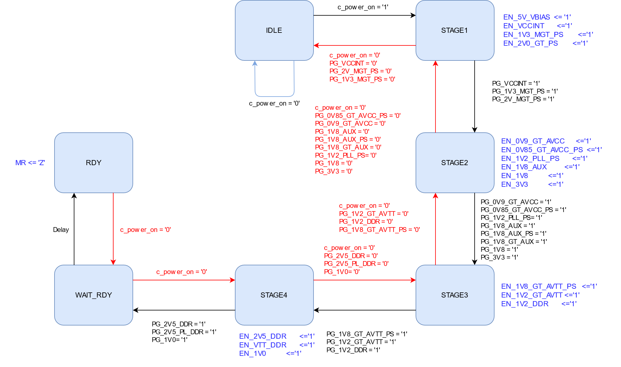
Power
In this board the CPLD is responsible for controlling and monitoring of output voltage and temperature of regulators and DC-DC converters. To control every converter chip or regualtor the CPLD monitors power good signal of regulators or DC-DC converters continuously to avoid over-voltage in the power system.
|
|
|
I2C
The main interface in the system is I2C interface. The user can input the data in the system through i2c slave subsystem. The entered data is stored in RAM memory. The state machine reads the stored data and communicates with corresponding sensor through i2c master subsystem and stores the feedback data again in RAM memory. The user can read back reported data for example temperature value.
|
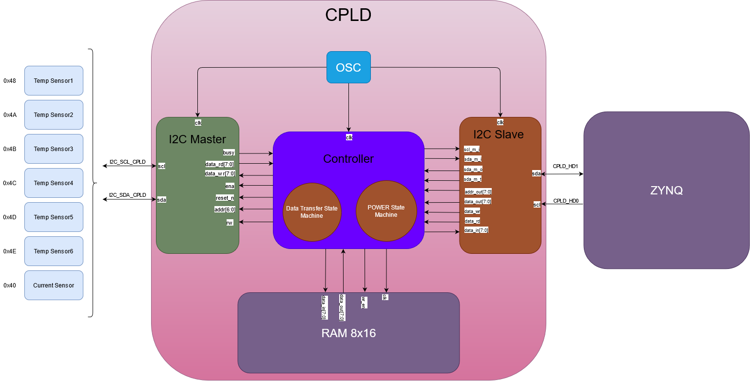
Internal Registers
Ram memory is a 16x8 Byte Memory.
|
The memory consists of the following registers:
- config_reg
- sensor_addr
- pointer_reg_byte
- data_to_write
- state_reg
- data_to_read
Sensor_addr register consists of sensor address that the temperature should be read from. Pointer_reg_byte is sensor internal register address that is to be written to or read from. Data_to_write register consists of data that in pointer_reg_byte will be written. The readed data from sensor is saved in data_to_read register. As long as state machine is busy , it will be state_teg value equal to 0x01. Config_reg consists of control bits. To start data transfer in state machine start_bit must be set to 1. If write_bit set to one, the inhalt of data_to_write will be written in pointer_reg_byte register of sensor . To read the inhalt of pointer_reg_byte register of sensor the read_bit must be set to 1.
Transfer state machine
To manage data transfer between RAM memory and i2c master subsystem that is connected with sensors, it is necessary to design a state machine. This state machine will be controlled with control bits of config_reg register. If start_bit is activated, state machine begins to transfer data between RAM memory and i2c master subsystem. If write_bit is set to one, saved data in RAM memory will be written in temperature sensor. If read_bit is set to one, temperature value will be readed from sensor and will be saved in RAM memory. Every state in the state machine consists of a state machine to manage i2c master communications.
In the following diagram this state machine construction is shown:
|
Sensors on board
|
All temperature sensors are TMP461 of texas instruments. When this sensor is in shutdown mode, a single conversion is started by writing any value in one_shot_start register ( poniter address 0x0F). The device returns to shutdown mode when the conversion and cycle completes. The result value is saved in high and low byte of Local/ Remote temperature registers. The high byte consists of temperature integer value and low byte consists of fraction part of temperature value. (Pointer addresses 0x00,0x15 for local temperature register and pointer addresses 0x01,0x10 for remote temperature register). The channel enable register (read address 16h, write address 16h) enables or disables the temperature conversion of remote and local temperature sensors. LEN (bit 0) of the channel enable register enables/disables the conversion of local temperature. REN (bit 1) of the channel enable register enables/disables the conversion of remote temperature. Both LEN and REN are set to 1 (default), this enables the ADC to convert both local and remote temperatures.
The TMP461 device is a digital temperature sensor that combines a local temperature measurement channel and a remote-junction temperature measurement channel in a single WQFN-10 package. The device is two-wire and SMBus-interface-compatible with nine pin-programmable bus address options, and is specified over a temperature range of –40°C to 125°C. The TMP461 device also contains multiple registers for programming and holding configuration settings, temperature limits, and temperature measurement results. In the following it is listed important registers of this sensor:
STATUS REG---------------------------------------Addr ---> 0x02 (read only) (Default N/A)
Local temperature register MSB 8 bits---------Addr ---> 0x00 (read only) (Default 0x00)
Local temperature register LSB 4 bits----------Addr ---> 0x15 (read only) (Default 0x00)
Remote temperature register MSB 8 bits------Addr ---> 0x01 (read only) (Default 0x00)
Remote temperature register LSB 4 bits-------Addr ---> 0x10 (read only) (Default 0x00)
Configuration register---------------------------Addr ---> 0x03 (read/write) (Default 0x00)
Channel enable register-------------------------Addr ---> 0x16 (read/write) (Default 0x03)
Conversion rate register------------------------Addr ---> 0x04 (read/write) (Default 0x08)
One-shot start register--------------------------Addr ---> 0x0F (read/write) (Default N/A)
The INA219 is a high-side current shunt and power monitor with an I2C interface. The INA219 monitors both shunt drop and supply voltage, with programmable conversion times and filtering. A programmable calibration value, combines with an internal multiplier, enables direct readouts in amperes. An additional multiplying register calculates power in watts. The I2C interface features 16 programmable accesses.
To access these sensors through ZynqMP can be executed the following instructions in linux console consecutively:
- Write device address
i2cset -y 2 0x20 0x01 <sensor address> --> This command writes sensor address in RAM memory address 0x01 (sensor_addr register)
- Write register address
i2cset -y 2 0x20 0x02 <register address> --> This command writes desired register address in RAM memory address 0x02 (pointer_reg_byte register)
- Write data that should be written in the register
i2cset -y 2 0x20 0x03 <data to write> --> This command writes desired value in RAM memory address 0x03 (data_to_write register)
- Start to write data
i2cset -y 2 0x20 0x00 0x03 --> This command set write_bit to one. (Write command)
- Stop writing data
i2cset -y 2 0x20 0x00 0x00 --> This command stops writing in RAM memory.
- Start to read data
i2cset -y 2 0x20 0x00 0x05 --> This command set read_bit to one. (Read command)
- Stop reading data
i2cset -y 2 0x20 0x00 0x00 --> This command stops reading from RAM memory.
- Read data_to_read register
i2cget -y 2 0x20 <data to read> --> This command reads data from desired register.
For example to read a temperature sensor it is necessary to give the following commands in linux console:
i2cset -y 2 0x20 0x01 <sensor address> --> Writing device address
i2cset -y 2 0x20 0x02 0x0F --> Writing One-shot register address
i2cset -y 2 0x20 0x03 0xFF --> Writing any value in the register to start converting of ADC in sensor
i2cset -y 2 0x20 0x00 0x03 --> Start to write these values
i2cset -y 2 0x20 0x00 0x00 --> To turn i2c master data transfer off
i2cset -y 2 0x20 0x02 0x00 --> Writing address of local temperature high byte register that consists of the temperature value
i2cset -y 2 0x20 0x00 0x03 --> Start to write these values
i2cset -y 2 0x20 0x00 0x00 --> To turn i2c master data transfer off
i2cset -y 2 0x20 0x00 0x05 --> Start to read temperature value of sensor and save it in data_to_read register
i2cset -y 2 0x20 0x00 0x00 --> To turn i2c master data transfer off
i2cget -y 2 0x20 0x09 --> Reading temperature value from data_to_read register
i2cset -y 2 0x20 0x02 0x15 --> Writing address of local temperature low byte register that consists of fraction of the temperature value
i2cset -y 2 0x20 0x00 0x03 --> Start to write these values
i2cset -y 2 0x20 0x00 0x00 --> To turn i2c master data transfer off
i2cset -y 2 0x20 0x00 0x05 --> Start to read temperature value of sensor and save it in data_to_read register
i2cset -y 2 0x20 0x00 0x00 --> To turn i2c master data transfer off
i2cget -y 2 0x20 0x09 --> Reading temperature fraction value from data_to_read register
If the following shell script is executed in linux console it can be read all temperatures of all temperature sensors on the board. This script file will be executed automatically while booting, if this file is copied to SD card.
#!/bin/sh

set sensor_addr=0                       # Temperature = Temp+Fraction*16^-1 °C for example 50+1*16^-1 = 50.0625 °C
Temp=0                                  # 8bits
Fraction=0                              # 4bits
i=0
n1=0
n2=0
for sensor_addr in 0x48 0x4A 0x4B 0x4C 0x4D 0x4E
do
        echo "Sensor Address $sensor_addr:"
        echo "Reading Sensor $i:"
        i2cset -y 2 0x20 0x01 $sensor_addr          # Write sensor address in RAM memory address 0x01
        i2cset -y 2 0x20 0x02 0x0F                  # Write one-shot-start register address in 0x02 of RAM
        i2cset -y 2 0x20 0x03 0xFF                  # Write 0xFF value in 0x03 address of RAM
        i2cset -y 2 0x20 0x00 0x03                  # Writing in sensor
        i2cset -y 2 0x20 0x00 0x00                  # Stop writing
        i2cset -y 2 0x20 0x02 0x00                  # Write 0x00 value (local temperature register high byte address) in 0x02 of RAM memory
        i2cset -y 2 0x20 0x00 0x03                  # Writing in sensor
        i2cset -y 2 0x20 0x00 0x00                  # Stop writing
        i2cset -y 2 0x20 0x00 0x05                  # Reading sensor
        i2cset -y 2 0x20 0x00 0x00                  # Stop reading
        Temp=`i2cget -y 2 0x20 0x09`                # Read temperature value stored in 0x09 address of RAM memory
        #echo $Temp
        n1=$(($Temp))
        #echo $n1
        i2cset -y 2 0x20 0x02 0x15                  # Write 0x15 value (local temperature register low byte address) in 0x02 of RAM memory
        i2cset -y 2 0x20 0x00 0x03                  # Writing in sensor
        i2cset -y 2 0x20 0x00 0x00                  # Stop writing
        i2cset -y 2 0x20 0x00 0x05                  # Reading sensor
        i2cset -y 2 0x20 0x00 0x00                  # Stop reading
        Fraction=`i2cget -y 2 0x20 0x09`            # Read temperature value stored in 0x09 address of RAM memory
        #echo $Fraction
        n2=$((Fraction>>4))                         # Shift bits 4 times
        #echo $n2
        echo "-----------------------------"
        #printf "Sensor %d Temperature = %d Celsius \n" $i $Temp
        #printf "Sensor %d Fraction = %d \n" $i $Fraction
        echo "Sensor $i Temperature = "
        awk "BEGIN {print  $n1+$n2*16**-1}"
        echo "Celsius"
        echo "-----------------------------"
        let i++
done |
|

LED
Green LED
|
RED LED
|
Appx. A: Change History and Legal Notices
Revision Changes
- Changes REV02 to REV03:
Added i2c slave to communicate with FPGA
Added i2c master to read and write temperature sensors value
Added i2c master state machine to manage communication between CPLD and temp. sensors
Added a 8x16 byte RAM to save data in RAM
- Correction of power sequencing
- Changes REV01 to REV02:
- Power Management
- FAN enable
- LED blink sequencing
- Changes REV00 to REV01:
- Power on (min)
- UART
- JTAG
Document Change History
To get content of older revision got to "Change History" of this page and select older document revision number.
|
| Date | Document Revision | CPLD Firmware Revision | Supported PCB Revision | Authors | Description |
|---|---|---|---|---|---|
| REV03 | REV02, REV03 |
| |||
| 2021-02-16 | v.39 | REV02 | REV02, REV03 | Mohsen Chamanbaz |
|
| All |
Legal Notices
|
|