Template Change history:
|
Important General Note:
|
----------------------------------------------------------------------- |
Note for Download Link of the Scroll ignore macro:
|
Overview
The Trenz Electronic TE0817 is an industrial grade MPSoC SoM integrating an AMD Zynq UltraScale+ MPSoC, DDR4 SDRAM with 64-Bit width data bus connection, SPI Boot Flash memory for configuration and operation, transceivers and powerful switch-mode power supplies for all on-board voltages. A large number of configurable I/Os is provided via rugged high-speed stacking connections in a compact 5.2 cm x 7.6 cm form factor.
Refer to http://trenz.org/te0817-info for the current online version of this manual and other available documentation.
Notes :
|
Key Features
Note: → See examples fro different types <Series Name> TRM Template section examples#%3CSeriesName%3ETRMTemplatesectionexamples-KeyFeatures |
|
Block Diagram
add drawIO object in Scroll Ignore section and add reference image in Scroll Only.
|
|
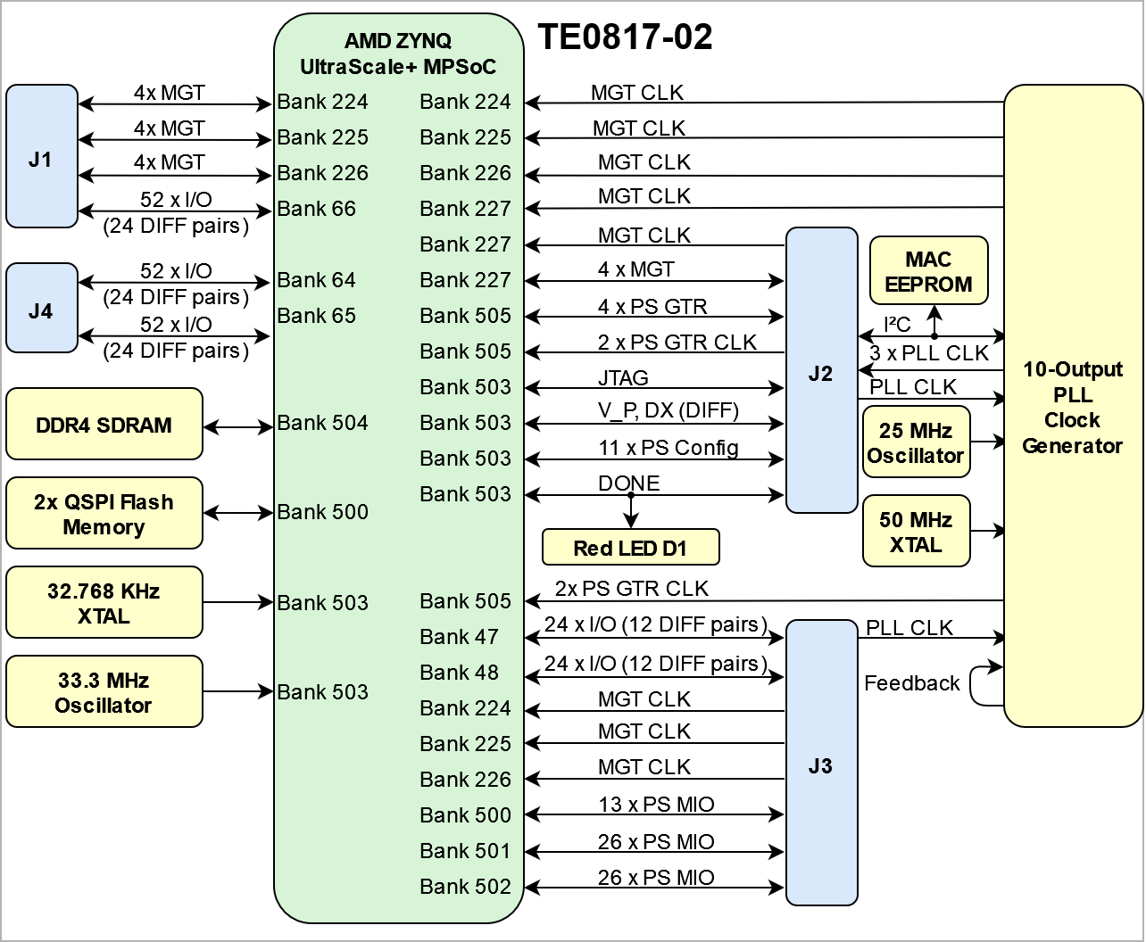

Main Components
Notes :
|
|
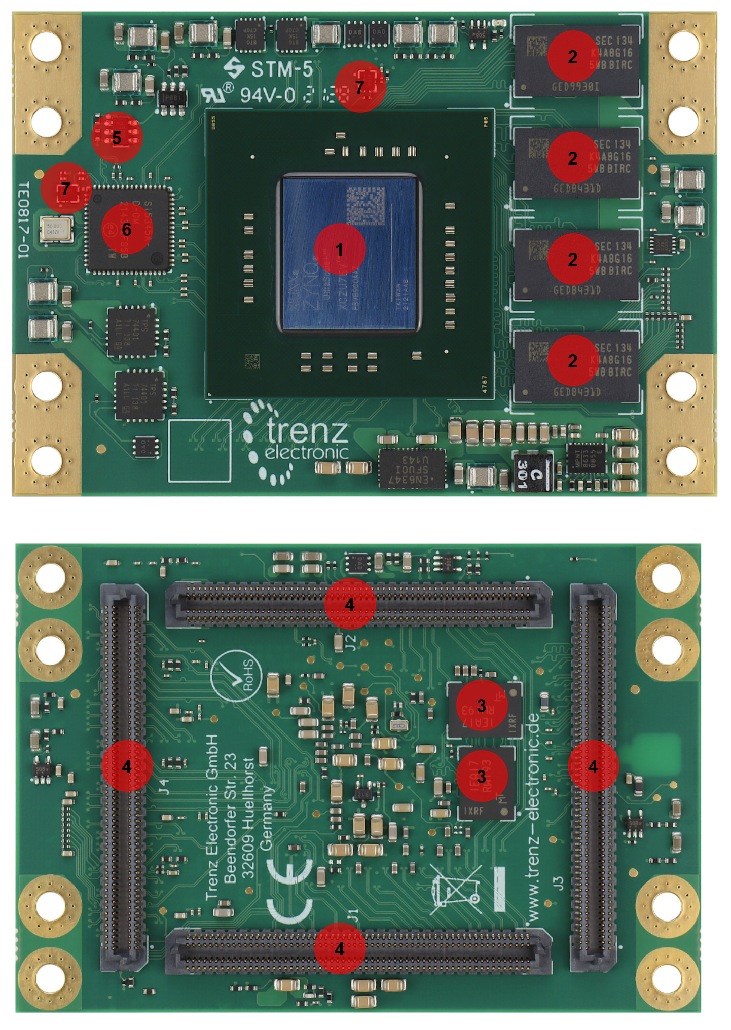

- SoC, U1
- DDR4, U2, U3, U9, U12
- Quad SPI Flash, U7, U17
- Connector, J1, J2, J3, J4
- EEPROM, U11
- Clock Generator, U5
- Oscillator, U25, U32
Initial Delivery State
|
|
Signals, Interfaces and Pins
For subsection examples see: <Series Name> TRM Template section examples#%3CSeriesName%3ETRMTemplatesectionexamples-Signals,InterfacesandPins
|
Connectors
1) IO CNT depends on assembly variant. E.g. the MGTs are not available for all FPGAs |
Test Points
you must fill the table below with group of Test Point which are indicated as TP in a schematic. If there is no Test Point remarked in the schematic, delet the Test Point section. Example:
1) Direction:
|
1) Test points depend on revision: Not all testpoints are available for all revisions. 2) Direction:
|
On-board Peripherals
Notes : In the on-board peripheral table "chip/Interface" must be linked to the corresponding chapter or subsection by assigning advance link using: #NameOfTheSection Example:
|
|
For example subsections see: <Series Name> TRM Template section examples#%3CSeriesName%3ETRMTemplatesectionexamples-On-boardPeripherals |
Configuration and System Control Signals
|
1) Direction:
2) See UG1085 for additional information. 3) See Recommended Operating Conditions. |
Power and Power-On Sequence
Enter the default value for power supply and startup of the module here.
Link to Schematics, for power images or more details |
Power Rails
List of all Powerrails which are accessible by the customer
|
1) Direction:
|
Recommended Power up Sequencing
List baseboard design hints for final baseboard development. |
The power up sequencing highly depends on the use case. In general, it should be possible to enable/disable the processing system (PS) / programmable logic (PL) independently. Furthermore, within the processing logic it should be possible to enable/disable only low-power domain and/or low-power and full-power domain. Additionally, usage of GTR for PS side and GTH for PL side should be possible. Because of this flexibility the needed parts of the following table needs to be selected individually. For detailed information take a look into schematics.
1) (optional) 2) Dependent on the assembly option a higher input voltage may be possible. 3) (on module) 4) This value depends highly on DCDC U4. Higher values may be possible with different DCDCs. For more information consult schematic and according datasheets. 5) See DS925 for additional information. | ||||||||||||||||||||||||||||||||||||||||||||||||||||||||||||||||||||||||||||||||||||||||||||||||||||||||||||||||||||||||||||||||||||||||||||||||||||||||||||||||||||||||||||||||||||||||||||||||
Board to Board Connectors
|
Technical Specifications
List of all Powerrails which are accessible by the customer
|
Absolute Maximum Ratings *)
1) For REV01 use max. 4 V instead which depends highly on DCDC U4. Higher values are possible with different DCDCs. For more information consult schematic and according datasheets. |
*) Stresses beyond those listed under Absolute Maximum Ratings may cause permanent damage to the device. These are stress ratings only, which do not imply functional operation of the device at these
or any other conditions beyond those indicated under Recommended Operating Condition. Exposure to absolute-maximum rated conditions for extended periods may affect device reliability.
Recommended Operating Conditions
This TRM is generic for all variants. Temperature range can be different depending on assembly version. Voltage range is mostly the same during variants (exceptions are possible, depending on custom request)
Operating temperature range depends also on customer design and cooling solution. Please contact us for options.
- Variants of modules are described here: Article Number Information
- Modules with commercial temperature grade are equipped with components that cover at least the range of 0°C to 75°C
- Modules with extended temperature grade are equipped with components that cover at least the range of 0°C to 85°C
- Modules with industrial temperature grade are equipped with components that cover at least the range of -40°C to 85°C
- The actual operating temperature range will depend on the FPGA / SoC design / usage and cooling and other variables.
1) Dependent on the assembly option a higher input voltage may be possible. 2) This value depends highly on REV01 DCDC U4. Higher values may possible with different DCDCs or different revision. For more information consult schematic and according datasheets. |
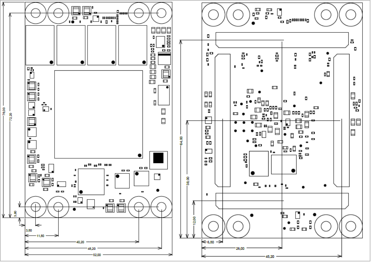
Physical Dimensions
Module size: 76 mm × 52 mm. Please download the assembly diagram for exact numbers.
Mating height with standard connectors: 5 mm.
PCB thickness: 1.74 mm (± 10 %).
In 'Physical Dimension' section, top and bottom view of module must be inserted, information regarding physical dimensions can be obtained through webpage for product in Shop.Trenz, (Download> Documents> Assembly part) for every SoM. For Example: for Module TE0728, Physical Dimension information can be captured by snipping tools from the link below:
|
|

Currently Offered Variants
Set correct link to the shop page overview table of the product on English and German. Example for TE0706: ENG Page: https://shop.trenz-electronic.de/en/search?sSearch=TE0813 DEU Page: https://shop.trenz-electronic.de/de/search?sSearch=TE0813 |
| ||||
Revision History
Hardware Revision History
Set correct links to download Carrier, e.g. TE0706 REV02: TE0706-02 -> https://shop.trenz-electronic.de/Download/?path=Trenz_Electronic/Modules_and_Module_Carriers/4x5/4x5_Carriers/TE0706/REV02/Documents Note:
|
|


|
Hardware revision number can be found on the PCB board together with the module model number separated by the dash.
Document Change History
|
|
Disclaimer
|
|