• Module: TRM Name always "TE Series Name" +TRM
    Example: "TE0728 TRM"

Template Change history:

DateVersionChangesAuthor

4.0
  • Rework for smaller TRM which can be generated faster
    • Reduce Signal Interfaces Pin
    • Reduce On Board Perihery
    • Reduce Power
    • Move Configuration Signals from Overview to own section
JH

3.12
  • Version History
    • changed from list to table
  • all
    • changed title-alignment for tables from left to center
ma

3.11
  • update "Recommended Operating Conditions" section


3.1
  • New general notes for temperature range to "Recommended Operating Conditions"


3.02
  • add again fix table of content with workaround to use it for pdf and wiki
  • Export Link for key features examples
    • Notes for different Types (with and without Main FPGA)
  • Export Link for Signals, Interfaces and Pins examples
    • Notes for different Types (Modul, Modul Hypride, Evalboard, Carrier)


3.01
  • remove fix table of content and page layout ( split page layout make trouble with pdf export)
  • changed and add note to signal and interfaces, to on board periphery section
  • ...(not finished)


3.00
  • → separation of Carrier/Module and evaluation kit TRM


2.15
  • add excerpt macro to key features


2.14
  • add fix table of content
  • add table size as macro


Important General Note:

  • If some section is configurable and depends on Firmware, please refer to the addition page (for example CPLD). If not available, add note, that this part is configurable
  • Designate all graphics and pictures with a number and a description, Use "Scroll Title" macro

    • Use "Scroll Title" macro for pictures and table labels. Figure number must be set manually at the moment (automatically enumeration is planned by scrollPDF)
      • Figure template:


        Create DrawIO object here: Attention if you copy from other page, objects are only linked.


        image link to the generate DrawIO PNG file of this page. This is a workaround until scroll pdf export bug is fixed


      • Table template:

        • Layout macro can be use for landscape of large tables

      • ExampleComment
        12


    • The anchors of the Scroll Title should be named consistant across TRMs. A incomplete list of examples is given below

      • <type>_<main section>_<name>

        • type: Figure, Table
        • main section:
          • "OV" for Overview
          • "SIP" for Signal Interfaces and Pins,
          • "OBP" for On board Peripherals,
          • "PWR" for Power and Power-On Sequence,
          • "B2B" for Board to Board Connector,
          • "TS" for Technical Specification
          • "VCP" for Variants Currently in Production
          •  "RH" for Revision History
        • name: custom, some fix names, see below
      • Fix names:
        • "Figure_OV_BD" for Block Diagram

        • "Figure_OV_MC" for Main Components

        • "Table_OV_IDS" for Initial Delivery State

        • "Table_PWR_PC" for Power Consumption

        • "Figure_PWR_PD" for Power Distribution
        • "Figure_PWR_PS" for Power Sequence
        • "Figure_PWR_PM" for Power Monitoring
        • "Table_PWR_PR" for Power Rails
        • "Table_PWR_BV" for Bank Voltages
        • "Table_TS_AMR" for Absolute_Maximum_Ratings

        • "Table_TS_ROC" for Recommended_Operating_Conditions

        • "Figure_TS_PD" for Physical_Dimensions
        • "Table_VCP_SO" for TE_Shop_Overview
        • "Table_RH_HRH" for Hardware_Revision_History

        • "Figure_RH_HRN" for Hardware_Revision_Number
        • "Table_RH_DCH" for Document_Change_History
    • Use Anchor in the document: add link macro and add "#<anchorname>
    • Refer to Anchror from external : <page url>#<pagename without space characters>-<anchorname>


-----------------------------------------------------------------------


Note for Download Link of the Scroll ignore macro:


Download PDF version of this document.

Overview

The Trenz Electronic AMB0010 is a commercial grade baseboard for Andromeda modules.

Refer to http://trenz.org/amb0010-info for the current online version of this manual and other available documentation.

Notes :

Key Features

Note:
 'description: Important components and connector or other Features of the module
→ please sort and indicate assembly options

See examples fro different types <Series Name> TRM Template section examples#%3CSeriesName%3ETRMTemplatesectionexamples-KeyFeatures


  • Module
    • Andromeda modules
  • On Board
    • 2 x B2B connector (ADF6)
    • Clock Buffer
    • Oscillator
  • Interface
    • RJ45 LAN Socket
    • XMOD
    • UART Header
    • I2C Header
    • 4 x User DIP Switch
    • 4 x User LED
    • Micro SD Card Socket with ESD protection
    • USB Connector
    • Loopbacks for GTHs, IOs, GPIOs
  • Power
    • 12 V Input Supply Voltage
  • Dimension
    • 128 mm x 106 mm

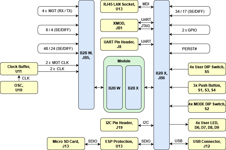
Block Diagram

add drawIO object in Scroll Ignore section and add reference image in Scroll Only.

For more information regarding how to draw a diagram, Please refer to "Diagram Drawing Guidline" .


Title (not anchor) of all Scroll Title such as DrawIOs and Tables should be changed according to the Module name.

Example: TE0812 Block Diagram


All created DrawIOs  should be named according to the Module name:

Example: DrawIO of TE0812 Block Diagram should be named TE0812_OV_BD


Main Components

Notes :

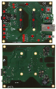
  • Picture of the PCB (top and bottom side) with labels of important components
  • Add List below


For more information regarding how to add board photoes, Please refer to "Diagram Drawing Guidline" .


  1. B2B Connector (ADF6), JB5, JB6
  2. Power Jack, J1
  3. Push Button, S1, S3, S4
  4. DIP Switch, S2, S5
  5. LED, D3...9
  6. Pin Header, J8, J19
  7. ESD Protection, U13
  8. Micro SD Socket, J13
  9. XMOD Connector, JB1
  10. RJ45 LAN Socket, J11
  11. USB Socket, J12

Initial Delivery State


Only components like EEPROM, QSPI flash can be initialized by default at manufacture.

If there is no components which might have initial data ( possible on carrier) you must keep the table empty


Storage device name

Content

Notes

-

-

-


Signals, Interfaces and Pins

For subsection examples see: <Series Name> TRM Template section examples#%3CSeriesName%3ETRMTemplatesectionexamples-Signals,InterfacesandPins

  • Table with all connectors and Designtor
  • List of different interfaces per connector
  • IO CNT (for FPGA IOs where functionality can be changed by customer)


Connectors

Connector TypeDesignatorInterfaceIO CNTNotes
B2BJB5HP104 SE / 48 DIFF
B2BJB5MGT PL4 x MGT (RX/TX)
B2BJB5MGT PL2 x MGT CLK
B2BJB5HD24 SE / 12 DIFF
B2BJB6HP52 SE / 24 DIFF
B2BJB6MGT PS4 x MGT (RX/TX)
B2BJB6MGT PS2 x MGT CLK
B2BJB6HD24 SE / 12 DIFF
B2BJB6MIO2 x I2C
B2BJB6MIO2 x UART
B2BJB6MIO2 x PERST
B2BJB6MIOSDIO
B2BJB6MIOJTAG
B2BJB6MIO4 x GPIO
B2BJB6ETH

B2BJB6USB

RJ45J11ETH

XMODJB1JTAGJTAG
XMODJB1UARTUART
Pin HeaderJ8UARTUART
Pin HeaderJ19I2CI2C
Power JackJ1PWRPWR
SD Card SocketJ13SDIOSDIO
USB SocketJ12USBUSB


Test Points

you must fill the table below with group of Test Point which are indicated as TP in a schematic. If there is no Test Point remarked in the schematic, delet the Test Point section.

Example:

Test PointSignalB2BNotes
10PWR_PL_OKJ2-120


Test PointSignalConnected toNotes
TP1+12.0V_input

TP2+12.0V_input

TP3V_MOD1
C2M
TP4V_MOD1
C2M
TP5Carrier_+3V3
C2M
TP6Carrier_+3V3
C2M
TP7Carrier_+1V8
C2M
TP8Carrier_+1V8
C2M
TP9Module_+3.3VJB6, U4M2C
TP10Module_+3.3VJB6, U4M2C
TP11Module_+1.8VJB5, JB6M2C
TP12Module_+1.8VJB5, JB6M2C
TP13PWR_ENJB6, S4PWR_EN is pulled-up in module AM0010 to 3.3 V.
TP14PWR_ENJB6, S4PWR_EN is pulled-up in module AM0010 to 3.3 V.
TP15Carrier_USB+5V

TP16Carrier_USB+5V

TP17PG_Carrier_+1V8U2, U3, U4, U5, U6, U7, U12
TP18PG_Carrier_+1V8U2, U3, U4, U5, U6, U7, U12
TP19Carrier_PGU3, U6, T7 (LED D5)
TP20Carrier_PGU3, U6, T7 (LED D5)
TP21PG_Carrier_USB+5VU7, U12
TP22PG_Carrier_USB+5VU7, U12
TP23PWR_GOODJB6, U4M2C, pulled-up in module AM0010 to 3.3 V.
TP24PWR_GOODJB6, U4M2C, pulled-up in module AM0010 to 3.3 V.
TP25USB-VBUS

TP26USB-VBUS

TP27IO_X0_D12_PJB6
TP28IO_X0_D12_PJB6
TP29M_SDAJB6
TP30M_SDAJB6
TP31M_SCLJB6
TP32M_SCLJB6
TP33RST_M2C#JB6
TP34RST_M2C#JB6
TP35U_INTJB6
TP36U_INTJB6
TP37PS_POR#JB6, S3PS_POR# is pulled up in module AM0010 to Carrier_+3V3 (V_IO_CFG).
TP38PS_POR#JB6, S3PS_POR# is pulled up in module AM0010 to Carrier_+3V3 (V_IO_CFG).
TP39PS_SRST#JB6, S1PS_SRST# is pulled up in module AM0010 to Carrier_+3V3 (V_IO_CFG).
TP40PS_SRST#JB6, S1PS_SRST# is pulled up in module AM0010 to Carrier_+3V3 (V_IO_CFG).
TP41DX_PJB6
TP42DX_PJB6
TP43DX_NJB6
TP44DX_NJB6
TP45M_INTJB6
TP46M_INTJB6


On-board Peripherals

Notes :

In the on-board peripheral table "chip/Interface" must be linked to the corresponding chapter or subsection by assigning advance link using: #NameOfTheSection

Example:

Chip/InterfaceDesignatorConnected ToNotes
ETH PHYU10
  • B2B connector J1
  • SoC MIO
Gigabit ETH PHY


Chip/InterfaceDesignatorConnected ToNotes
OscillatorU10U11
Clock BufferU11JB5
RJ45 LAN SocketJ11JB6
XMODJB1JB6
Pin HeaderJ8JB6
Pin HeaderJ19JB6
Power JackJ1

Micro SD Card SocketJ13JB6 via U13
USB SocketJ12JB6 via L7


For example subsections see: <Series Name> TRM Template section examples#%3CSeriesName%3ETRMTemplatesectionexamples-On-boardPeripherals

Configuration and System Control Signals

  • Overview  all Controller signals, like Reset, Boote Mode, JTAG Interface(Connector or USB In case of FTDI)...
  • In case it's connected to CPLD always link to CPLD description and add not from the  current implementation here(in case it's available)


Connector+Pin

Signal Name

DirectionDescription
JB6.A59V_BATC2MInput voltage for VCC_PSBATT
JB6.B58RST_M2C#M2CModule reset for peripheral reset
JB6.C53DONEM2CFPGA PS_DONE-signal
JB6.C54MODE0C2MBoot mode selection
JB6.C55MODE1C2MBoot mode selection
JB6.C56MODE2C2MBoot mode selection
JB6.C57MODE3C2MBoot mode selection
JB6.C58PS_SRST#C2MFPGA system reset
JB6.C59PS_POR#bidirectionalPower-on-reset status
JB6.D56DX_PC2MTemperature sensing diode pin
JB6.D57DX_NC2MTemperature sensing diode pin
JB6.D58PWR_ENC2M

Power Enable
(Do not tie "PWR_EN" to VDD directly.
This signal could be tied to GND within
the AM0010 module.)

JB6.D59PWR_GOODM2CPower good status

Legend:

C2M: Carrier to Module

M2C: Module to Carrier

Power and Power-On Sequence

Enter the default value for power supply and startup of the module here.

  • Order of power provided Voltages and Reset/Enable signals

Link to Schematics, for power images or more details


Power Rails

List of all Powerrails which are accessible by the customer

  • Main Power Rails and Variable Bank Power


Power Rail Name/ Schematic NameConnector + PinDirectionNotes
V_MOD1JB5.A7C2M
V_MOD1JB5.A15C2M
V_MOD1JB5.A47C2M

V_MOD1

JB5.A55C2M
V_MOD1JB5.B5C2M
V_MOD1JB5.B11C2M
V_MOD1JB5.B17C2M
V_MOD1JB5.B45C2M
V_MOD1JB5.B51C2M
V_MOD1JB5.B57C2M
Module_+1.8VJB5.C7M2C
Module_+1.8VJB5.C15M2C
Carrier_+1V8JB5.D3C2M
Carrier_+1V8JB5.D17C2M
Carrier_+3V3JB5.D40C2M
Carrier_+1V8JB5.D43C2M
Carrier_+1V8JB5.D57C2M
Carrier_+1V8JB6.A3C2M
Carrier_+1V8JB6.A17C2M
Carrier_+1V8JB6.A59C2M
Module_+1.8VJB6.B7M2C
Module_+1.8VJB6.B15M2C
Carrier_+3V3JB6.B35C2M
Module_+3.3VJB6.B59M2C
V_MOD1JB6.C5C2M
V_MOD1JB6.C11C2M
V_MOD1JB6.C17C2M
Carrier_+3V3JB6.C52C2M
V_MOD1JB6.D7C2M
V_MOD1JB6.D15C2M
Carrier_+3V3JB1.5C2M
Carrier_+3V3JB1.6C2M
Carrier_+3V3J8.1C2M
Carrier_+3V3J19.1C2M
+12.0V_inputJ1.12M

Legend:

C2M: Carrier to Module

  2M: to Module

M2C: Module to Carrier

Board to Board Connectors

  • This section is optional and only for modules.
  • use "include page" macro and link to the general B2B connector page of the module series,

    For example: 6 x 6 SoM LSHM B2B Connectors

Technical Specifications

List of all Powerrails which are accessible by the customer

  • Main Power Rails and Variable Bank Power add boarder one time maximum Rating (Board will damaged)

Absolute Maximum Ratings


Power Rail Name/ Schematic NameDescriptionMinMaxUnit
+12.0V_inputPower Supply11.013.0V


Recommended Operating Conditions

This TRM is generic for all variants. Temperature range can be differ depending on the assembly version.  Voltage range is mostly the same during variants (exceptions are possible, depending on custom request)

Operating temperature range depends also on customer design and cooling solution. Please contact us for options.

  • Variants of modules are described here: Article Number Information
  • Modules with commercial temperature grade are equipped with components that cover at least the range of 0°C to 75°C
  • Modules with extended temperature grade are equipped with components that cover at least the range of 0°C to 85°C
  • Modules with industrial temperature grade are equipped with components that cover at least the range of -40°C to 85°C
  • The actual operating temperature range will depend on the FPGA / SoC design / usage and cooling and other variables.


Power Rail Name/ Schematic NameMinTypicalMaxUnitsReference Document
+12.0V_input11.012.013.0VSee LTC4365ITS8 datasheets.


Physical Dimensions

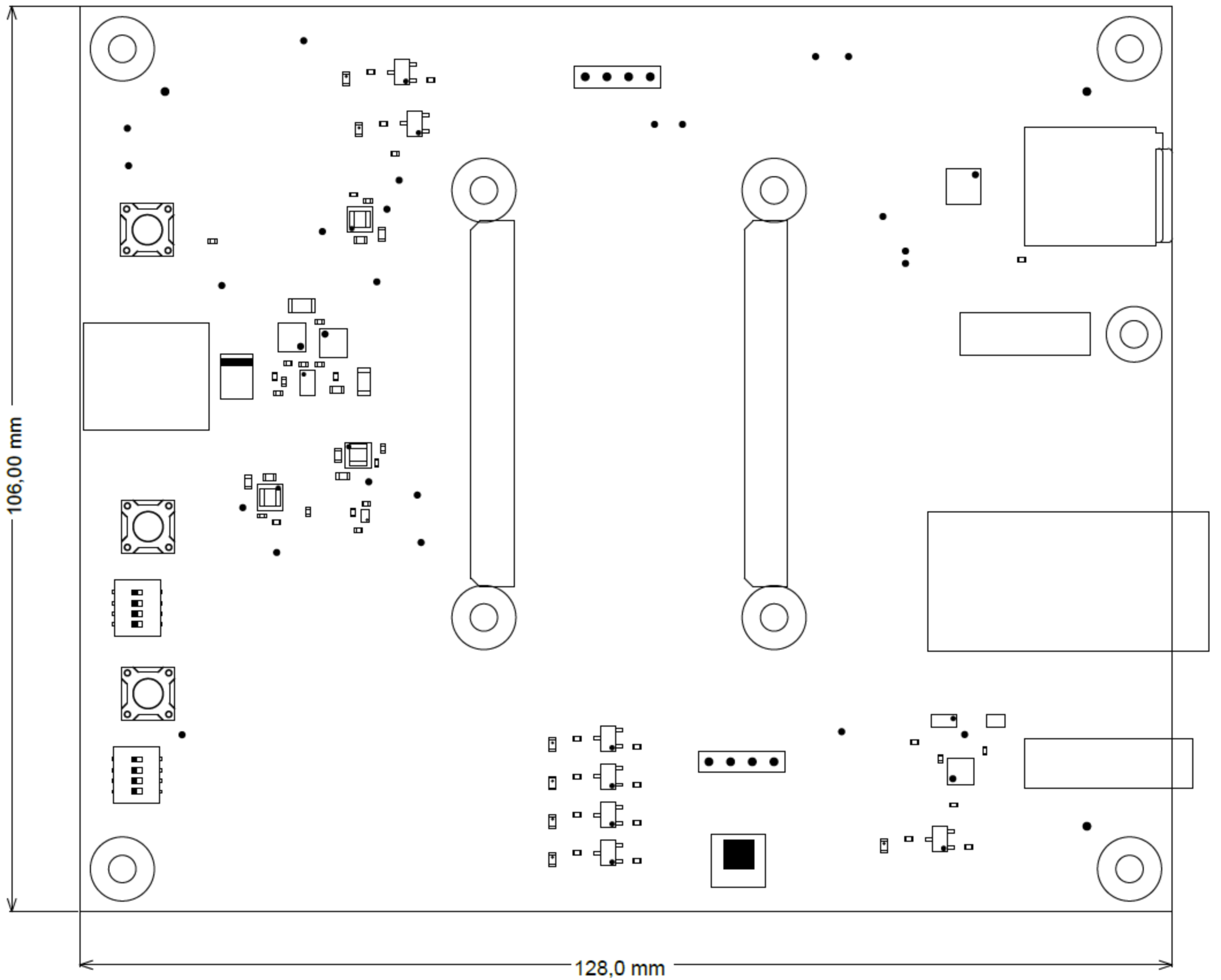
  • Module size: 128 mm × 106 mm.  Please download the assembly diagram for exact numbers.

  • Mating height with standard connectors: 5 mm.

PCB thickness: 1.6 mm.

In 'Physical Dimension' section, top and bottom view of module must be inserted, information regarding physical dimensions can be obtained through webpage for product in Shop.Trenz, (Download> Documents> Assembly part) for every SoM.

For Example: for Module TE0728, Physical Dimension information can be captured by snipping tools from the link below:

https://www.trenz-electronic.de/fileadmin/docs/Trenz_Electronic/Modules_and_Module_Carriers/5.2x7.6/TE0745/REV02/Documents/AD-TE0745-02-30-1I.PDF

For more information regarding how to draw diagram, Please refer to "Diagram Drawing Guidline" .


Currently Offered Variants 

Set correct link to the shop page overview table of the product on English and German.

Example for TE0706:

    ENG Page: https://shop.trenz-electronic.de/en/search?sSearch=TE0706

    DEU Page: https://shop.trenz-electronic.de/de/search?sSearch=TE0706


Trenz shop AMB0010 overview page
English pageGerman page


Revision History

Hardware Revision History

Set correct links to download  Carrier, e.g. TE0706 REV02:

  TE0706-02  ->   https://shop.trenz-electronic.de/Download/?path=Trenz_Electronic/Modules_and_Module_Carriers/4x5/4x5_Carriers/TE0706/REV02/Documents

Note:

  • Date format:  YYYY-MM-DD
  • Example: 

    DateRevisionChangesDocumentation Link
    2020-11-25REV02
    • Resistors R14 and R15 was replaced by 953R (was 5K1)
    • Resistor R5 was replaced by 5K1, R8 by 953R (was 9K09 and 1K69 respectively)
    REV02


DateRevisionChangesDocumentation Link
-REV01Initial Revision


Hardware revision number can be found on the PCB board together with the module model number separated by the dash.

Document Change History

  • Note this list must be only updated, if the document is online on public doc!
  • It's semi automatically, so do following
    • Add new row below first

    • Copy "Page Information Macro (date)" Macro-Preview, Metadata Version number, Author Name and description to the empty row. Important Revision number must be the same as the Wiki document revision number Update Metadata = "Page Information Macro (current-version)" Preview+1 and add Author and change description. --> this point is will be deleted on newer pdf export template

    • Metadata is only used of compatibility of older exports


DateRevisionContributorDescription

  • <add TRM change list here>

--

all

  • --


Disclaimer


<style>
.wiki-content .columnLayout .cell.aside {
width: 0%;
}</style>


Table of contents