• Module: TRM Name always "TE Series Name" +TRM
    Example: "TE0728 TRM"

Template Change history:

DateVersionChangesAuthor

4.2
  • Changes Xilinx to AMD
ED

4.1
  • Minor changes
    • Notes
    • Tables
ED

4.0
  • Rework for smaller TRM which can be generated faster
    • Reduce Signal Interfaces Pin
    • Reduce On Board Periphery
    • Reduce Power
    • Move Configuration Signals from Overview to own section
JH

3.12
  • Version History
    • changed from list to table
  • all
    • changed title-alignment for tables from left to center
ma

3.11
  • update "Recommended Operating Conditions" section


3.1
  • New general notes for temperature range to "Recommended Operating Conditions"


3.02
  • add again fix table of content with workaround to use it for pdf and wiki
  • Export Link for key features examples
    • Notes for different Types (with and without Main FPGA)
  • Export Link for Signals, Interfaces and Pins examples
    • Notes for different Types (Modul, Modul Hybrid, Evalboard, Carrier)


3.01
  • remove fix table of content and page layout ( split page layout make trouble with pdf export)
  • changed and add note to signal and interfaces, to on board periphery section
  • ...(not finished)


3.00
  • → separation of Carrier/Module and evaluation kit TRM


2.15
  • add excerpt macro to key features


2.14
  • add fix table of content
  • add table size as macro


Important General Note:

  • If some section is configurable and depends on Firmware, please refer to the addition page (for example CPLD). If not available, add note, that this part is configurable
  • Designate all graphics and pictures with a number and a description, Use "Scroll Title" macro

    • Use "Scroll Title" macro for pictures and table labels. Figure number must be set manually at the moment (automatically enumeration is planned by scrollPDF)
      • Figure template:


        Create DrawIO object here: Attention if you copy from other page, objects are only linked.


        image link to the generate DrawIO PNG file of this page. This is a workaround until scroll pdf export bug is fixed


      • Table template:

        • Layout macro can be use for landscape of large tables

      • ExampleComment
        12


    • The anchors of the Scroll Title should be named consistent across TRMs. A incomplete list of examples is given below

      • <type>_<main section>_<name>

        • type: Figure, Table
        • main section:
          • "OV" for Overview
          • "SIP" for Signal Interfaces and Pins,
          • "OBP" for On board Peripherals,
          • "PWR" for Power and Power-On Sequence,
          • "B2B" for Board to Board Connector,
          • "TS" for Technical Specification
          • "VCP" for Variants Currently in Production
          •  "RH" for Revision History
        • name: custom, some fix names, see below
      • Fix names:
        • "Figure_OV_BD" for Block Diagram

        • "Figure_OV_MC" for Main Components

        • "Table_OV_IDS" for Initial Delivery State

        • "Table_PWR_PC" for Power Consumption

        • "Figure_PWR_PD" for Power Distribution
        • "Figure_PWR_PS" for Power Sequence
        • "Figure_PWR_PM" for Power Monitoring
        • "Table_PWR_PR" for Power Rails
        • "Table_PWR_BV" for Bank Voltages
        • "Table_TS_AMR" for Absolute_Maximum_Ratings

        • "Table_TS_ROC" for Recommended_Operating_Conditions

        • "Figure_TS_PD" for Physical_Dimensions
        • "Table_VCP_SO" for TE_Shop_Overview
        • "Table_RH_HRH" for Hardware_Revision_History

        • "Figure_RH_HRN" for Hardware_Revision_Number
        • "Table_RH_DCH" for Document_Change_History
    • Use Anchor in the document: add link macro and add "#<anchorname>
    • Refer to Anchor from external : <page url>#<pagename without space characters>-<anchorname>


-----------------------------------------------------------------------


Note for Download Link of the Scroll ignore macro:


Download PDF version of this document.

Overview

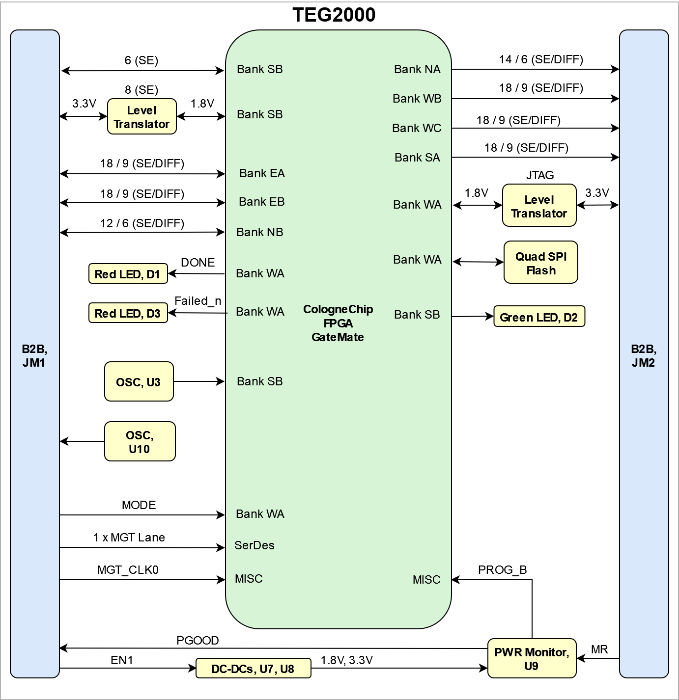
The Trenz Electronic TEG2000 is a FPGA module integrating a CologneChip GateMate FPGA, a QSPI Flash, level shifter, LEDs and several clocking and power components necessary for all on-board voltages. Numerous configurable I/Os are provided via rugged high-speed strips. All this on a tiny footprint, smaller than a credit card size at a very competitive price. All Trenz Electronic SoMs in 4 x 5 cm form factor are mechanically compatible.

Refer to http://trenz.org/teg2000-info for the current online version of this manual and other available documentation.

Notes :

Key Features

Note:
 'description: Important components and connector or other Features of the module
→ please sort and indicate assembly options

See examples for different types <Series Name> TRM Template section examples#%3CSeriesName%3ETRMTemplatesectionexamples-KeyFeatures


  • SoC/FPGA/Module
    • CologneChip GateMate A1 / A2 / A4 1)
    • performance mode: economy, speed 1)
    • Temperature range: industrial (-20°C to 85°C)
  • RAM/Storage
    • 16 MByte QSPI Flash 2) 
  • On Board
    • Oscillator

    • 3 x LED

    • Level shifter
  • Interface
    • 2 x B2B Connector (LSHM)

    • Configuration via Flash on board, USB or JTAG
    • 2.5 Gb/s SerDes interface
    • 2 x B2B Connector (LSHM)
      • up to 130 single ended IO / up to 57 differential pairs
      • JTAG
  • Power
    • 3.3 V power supply via B2B Connector needed

  • Dimension
    • 40 x 50 mm
  • Notes
    1) Please, take care of the possible assembly options. 
    2) Up to 16 MByte are possible.

Block Diagram

add drawIO object in Scroll Ignore section and add reference image in Scroll Only.

For more information regarding how to draw a diagram, Please refer to "Diagram Drawing Guidline" .


Title (not anchor) of all Scroll Title such as DrawIOs and Tables should be changed according to the Module name.

Example: TE0812 Block Diagram


All created DrawIOs  should be named according to the Module name:

Example: DrawIO of TE0812 Block Diagram should be named TE0812_OV_BD


Main Components

Notes :

  • Picture of the PCB (top and bottom side) with labels of important components
  • Add List below


For more information regarding how to add board photoes, Please refer to "Diagram Drawing Guidline" .


  1. CologneChip GateMate FPGA, U1
  2. QSPI Flash, U5
  3. Power Switch, Q1
  4. DCDC, U7, U8
  5. Power Monitor, U9
  6. Oscillator, U10, U3
  7. LEDs, D1, D2, D3
  8. B2B connector, JM2, JM1
  9. Level shifter, U2
  10. Optional additional Flash, U4
  11. BUS-Transceiver, U6

Initial Delivery State


Only components like EEPROM, QSPI flash can be initialized by default at manufacture.

If there is no components which might have initial data ( possible on carrier) you must keep the table empty


Storage device name

Content

Notes

Quad SPI Flash

Blinky Demo Design

U5


Signals, Interfaces and Pins

For subsection examples see: <Series Name> TRM Template section examples#%3CSeriesName%3ETRMTemplatesectionexamples-Signals,InterfacesandPins

  • Table with all connectors and Designator
  • List of different interfaces per connector
  • IO CNT (for FPGA IOs where functionality can be changed by customer)


Connectors

Connector TypeDesignatorInterfaceIO CNTNotes
B2B JM1SerDes8
B2B JM1GPIO48Bank NB/EB/EA, powered by VCCIOA
B2B JM1GPIO6up to 3.3V due to level shifter, connected to Bank SB
B2B JM1GPIO6up to 1.8V, also connected to Bank SB
B2B JM1configuration Signals3EN1, PGOOD , MODE
B2B JM2GPIO50Bank NA/WB/WC, powered by VCCIOD
B2B JM2GPIO18Bank SA, powered by VCCIOC
B2B JM2JTAG40..3.3VIN
B2B JM2MR1low active Reset
B2B JM1CLKDIFF CLK


Test Points

you must fill the table below with group of Test Point which are indicated as TP in a schematic. If there is no Test Point remarked in the schematic, delete the Test Point section.

Example:

Test PointSignalNotes1)
TP1PWR_PL_OK

1) Direction:

    • IN: Input from the point of view of this board.
    • OUT: Output from the point of view of this board.


Test PointSignalSideNotes1)
TP1NA_6_N TP1topFPGA IO
TP2NA_6_PtopFPGA IO
TP3NB_B3topFPGA IO
TP4NB_A3topFPGA IO
TP51Vbottom1V power rail
TP6DONEbottomFPGA CFG_DONE pin
TP7PROG_BbottomFPGA RST_N pin
TP8GNDbottom
TP9GNDbottom
TP101Vtop1V power rail
TP111.8V topOUT, 1.8V power rail
TP12VINtopVIN (3.3 - 5.0V)
TP133.3VINtop
TP143.3VtopOUT, 3.3V power rail
TP15VCCIOAtopIN 1.1V ... 2.7V, powers IO Banks NB/EB/EA
TP16VCCIOCtopIN 1.1V ... 2.7V, powers IO Bank SA
TP17VCCIODtopIN 1.1V ... 2.7V, powers IO Banks NA/WB/WC
TP18DONEtopFPGA CFG_DONE pin
TP19PROG_BtopFPGA RST_N pin
TP20GNDtop
TP21GNDtop
TP22FAILED_nbottomFPGA CFG_FAILED pin
TP23FAILED_ntopFPGA CFG_FAILED pin

1) Direction:

    • IN: Input from the point of view of this board.
    • OUT: Output from the point of view of this board.

On-board Peripherals

Notes :

In the on-board peripheral table "chip/Interface" must be linked to the corresponding chapter or subsection by assigning advance link using: #NameOfTheSection

Example:

Chip/InterfaceDesignatorConnected ToNotes
ETH PHYU10
  • B2B connector J1
  • SoC MIO
Gigabit ETH PHY


Chip/InterfaceDesignatorConnected ToNotes

QSPI Flash

U5FPGA Bank CFG WASPIx4 Interface for FPGA configuration

Oscillator

U3FPGA Bank SB, Pin IO_SB_A825 MHz

Oscillator

U10JM1.16, JM1.18differential 100 MHz Clock for Gigabit-Transceiver


For example subsections see: <Series Name> TRM Template section examples#%3CSeriesName%3ETRMTemplatesectionexamples-On-boardPeripherals

Configuration and System Control Signals

  • Overview  all Controller signals, like Reset, Boote Mode, JTAG Interface(Connector or USB In case of FTDI)...
  • In case it's connected to CPLD always link to CPLD description and add not from the  current implementation here(in case it's available)


Connector+Pin

Signal Name

Direction1)Description
JM1.28EN1INactivates DC-DCs
JM1.30PGOODOUTOutput from power monitor
JM1.32MODEINconfiguration mode -
0 → JTAG or 1 → SPI active Mode
JM2.18MRINlow active Reset connected to the Power Monitor that triggers PROG_B (FPGA RST_N)

JM2.93 / JM2.95 /

JM2.97 / JM2.99

TMS / TDI / TDO / TCKSignal-dependent

JTAG configuration and debugging interface.

JTAG reference voltage: 3.3V

1) Direction:

    • IN: Input from the point of view of this board.
    • OUT: Output from the point of view of this board.

Power and Power-On Sequence

Enter the default value for power supply and startup of the module here.

  • Order of power provided Voltages and Reset/Enable signals

Link to Schematics, for power images or more details


Power Rails

List of all power rails which are accessible by the customer

  • Main Power Rails and Variable Bank Power


Power Rail Name/ Schematic NameConnector + PinDirection1)Notes
VINJM1.1 / JM1.3 / JM1.5 / JM2.2 / JM2.4 / JM2.6 / JM1.8 IN3.3 V - 5.0V, Micromodule Power
3.3VINJM1.13 / JM1.15INMicromodule Power
VCCIOAJM1.9 / JM1.11IN
VCCIOCJM2.5IN
VCCIODJM2.7 / JM2.9IN
3.3V

JM2.10 / JM2.12 / JM2.91

OUTPower for Carrier, powers on module the level shifter, LEDs and control Pins
1.8VJM1.39OUTPower for Carrier, On module it powers the Flash, FPGA VDD and Banks SB,WA
1V----Powers the FPGA core, PLLs and SerDes interface

1) Direction:

    • IN: Input from the point of view of this board.
    • OUT: Output from the point of view of this board.

Recommended Power up Sequencing

List baseboard design hints for final baseboard development.


SequenceNet nameRecommended Voltage RangePull-up/downDescriptionNotes
0---Configuration signal setup.See Configuration and System Control Signals.
1VIN3.3 V - 5.0 V (± 5 %)-Main power supply
1EN1-PU 1), 3.3VINpower enable
1PGOOD-PU 1), 3.3Vpower good status.
23.3VIN3.3 V (± 5 %)-Main power supplyMain module power supply. 0.5 A minimum. Power consumption depends mainly on design and cooling solution.
3VCCIOA, VCCIOC, VCCIOD1.1 V - 2.7 V-Bank Voltages1.8 V on TE0703 Carrier

1) (on module)

Board to Board Connectors

  • This section is optional and only for modules.
  • use "include page" macro and link to the general B2B connector page of the module series,

    For example: 4 x 5 SoM LSHM B2B Connectors


Technical Specifications

List of all power rails which are accessible by the customer

  • Main Power Rails and Variable Bank Power add boarder one time maximum Rating (Board will damaged)

Absolute Maximum Ratings *)

Power Rail Name/ Schematic NameDescriptionMinMaxUnit
VINMicromodule Power-0.36.5V
3.3VINMicromodule Power-0.36.5V
VCCIOABank NB/EB/EA voltage-2.75V
VCCIOC Bank SA voltage-2.75V
VCCIODBank NA/WB/WC voltage-2.75V


*) Stresses beyond those listed under Absolute Maximum Ratings may cause permanent damage to the device. These are stress ratings only, which do not imply functional operation of the device at these
   or any other conditions beyond those indicated under Recommended Operating Condition. Exposure to absolute-maximum rated conditions for extended periods may affect device reliability.

Recommended Operating Conditions

This TRM is generic for all variants. Temperature range can be differ depending on the assembly version.  Voltage range is mostly the same during variants (exceptions are possible, depending on custom request)

Operating temperature range depends also on customer design and cooling solution. Please contact us for options.

  • Variants of modules are described here: Article Number Information
  • Modules with commercial temperature grade are equipped with components that cover at least the range of 0°C to 75°C
  • Modules with extended temperature grade are equipped with components that cover at least the range of 0°C to 85°C
  • Modules with industrial temperature grade are equipped with components that cover at least the range of -40°C to 85°C
  • The actual operating temperature range will depend on the FPGA / SoC design / usage and cooling and other variables.
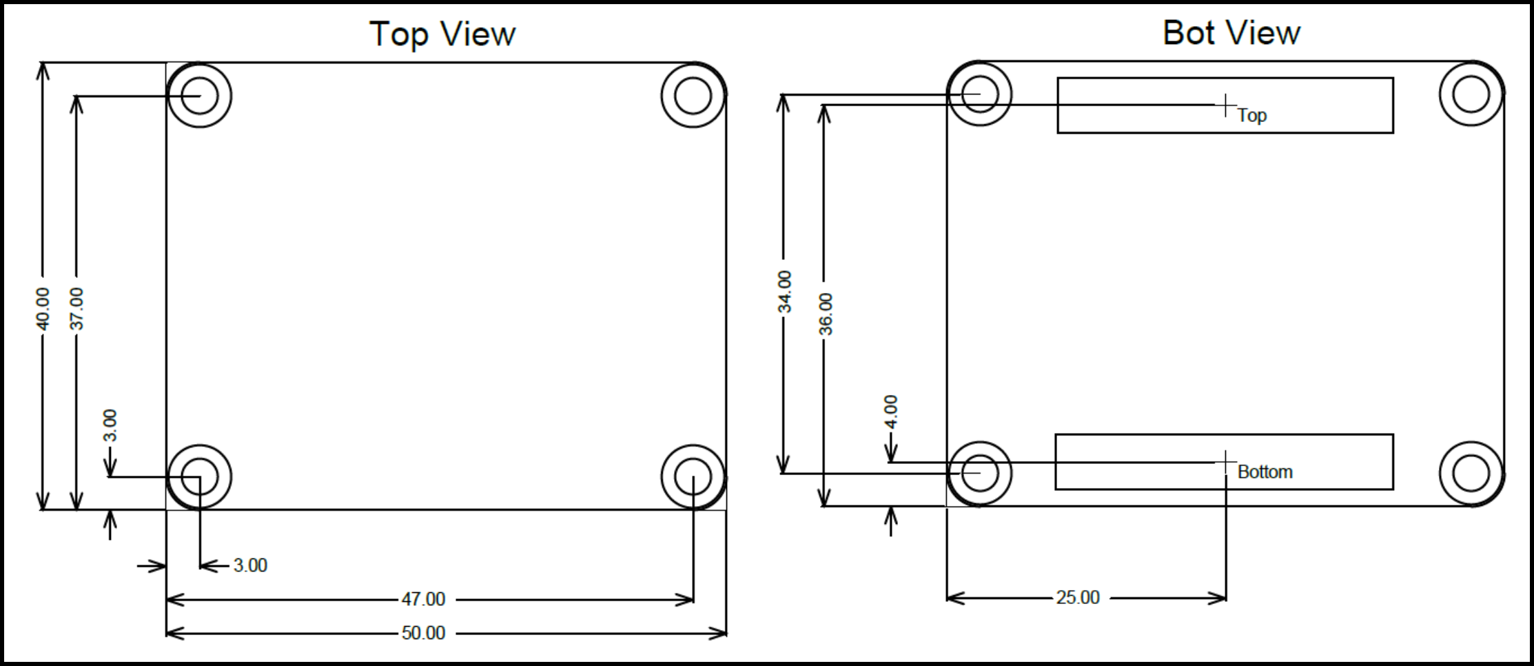

ParameterMinMaxUnitsReference Document
VIN3,1355,25V
3.3VIN3,1353,465V
VCCIOA1.12.75V
VCCIOC 1.12.75V
VCCIOD1.12.75V


Physical Dimensions

  • Module size: 40 mm × 50 mm.  Please download the assembly diagram for exact numbers.

  • Mating height with standard connectors: 8 mm.

PCB thickness: 1.4 mm.

All dimensions are shown in millimeters.

In 'Physical Dimension' section, top and bottom view of module must be inserted, information regarding physical dimensions can be obtained through webpage for product in Shop.Trenz, (Download> Documents> Assembly part) for every SoM.

For Example: for Module TE0728, Physical Dimension information can be captured by snipping tools from the link below:

https://www.trenz-electronic.de/fileadmin/docs/Trenz_Electronic/Modules_and_Module_Carriers/5.2x7.6/TE0745/REV02/Documents/AD-TE0745-02-30-1I.PDF

For more information regarding how to draw diagram, Please refer to "Diagram Drawing Guideline" .


Currently Offered Variants 

Set correct link to the shop page overview table of the product on English and German.

Example for TE0706:

    ENG Page: https://shop.trenz-electronic.de/en/search?sSearch=TE0706

    DEU Page: https://shop.trenz-electronic.de/de/search?sSearch=TE0706


Trenz shop TEG2000 overview page
English pageGerman page


Revision History

Hardware Revision History

Set correct links to download  Carrier, e.g. TE0706 REV02:

  TE0706-02  ->   https://shop.trenz-electronic.de/Download/?path=Trenz_Electronic/Modules_and_Module_Carriers/4x5/4x5_Carriers/TE0706/REV02/Documents

Note:

  • Date format:  YYYY-MM-DD
  • Example: 

    DateRevisionChangesDocumentation Link
    2020-11-25REV02
    • Resistors R14 and R15 was replaced by 953R (was 5K1)
    • Resistor R5 was replaced by 5K1, R8 by 953R (was 9K09 and 1K69 respectively)
    REV02


DateRevisionChangesDocumentation Link
-REV01

First Production Release

REV01


Hardware revision number can be found on the PCB board together with the module model number separated by the dash.

Document Change History

  • Note this list must be only updated, if the document is online on public doc!
  • It's semi automatically, so do following
    • Add new row below first

    • Copy "Page Information Macro (date)" Macro-Preview, Metadata Version number, Author Name and description to the empty row. Important Revision number must be the same as the Wiki document revision number Update Metadata = "Page Information Macro (current-version)" Preview+1 and add Author and change description. --> this point is will be deleted on newer pdf export template

    • Metadata is only used of compatibility of older exports


DateRevisionContributorDescription

  • initial revision

--

all

  • --


Disclaimer


<style>
.wiki-content .columnLayout .cell.aside {
width: 0%;
}</style>


Table of contents