Design Name always "TE Series Name" + optional CPLD Name + "CPLD"
|
Overview
CPLD Device with designator U14: LCMX02-1200HC
Feature Summary
- Power Management
- Reset Management
- Boot Mode Controller
- FPGA UART routing
- I2C to GPIO
Firmware Revision and supported PCB Revision
Product Specification
Port Description
| Name / opt. VHD Name | Direction | Pin | Pull up/ down | Bank Power | Description |
|---|---|---|---|---|---|
| ACBUS4 | in | 96 | UP | 3.3V | FTDI / It can be read via i2c to GPIO. ( GPIO_input(22) ) |
| ACBUS5 | in | 88 | UP | 3.3V | FTDI / It can be read via i2c to GPIO. ( GPIO_input(23) ) |
| ADBUS4 | out | 98 | NONE | 3.3V | FTDI / M_TCK is connected to ADBUS4. |
| ADBUS7 | out | 97 | UP | 3.3V | FTDI / currently_not_used |
| BDBUS0 | inout | 87 | NONE | 3.3V | FTDI / Module UART0-RX << FTDI |
| BDBUS1 | inout | 86 | NONE | 3.3V | FTDI /Module UART0-TX >> FTDI |
| C_TCK | out | 81 | DOWN | 3.3V | TCK JTAG port pin connected to Module |
| C_TDI | out | 84 | DOWN | 3.3V | TDI JTAG port pin connected to Module |
| C_TDO | in | 83 | DOWN | 3.3V | TDO JTAG port pin connected to Module |
| C_TMS | out | 85 | UP | 3.3V | TMS JTAG port pin connected to Module |
| CM0 | in | 67 | UP | 3.3V | DIP Switch S3-M1 / Used to select FMC_VADJ voltage |
| CM1 | in | 66 | UP | 3.3V | DIP Switch S3-M2 / Used to select FMC_VADJ voltage |
| EN_FMC | out | 35 | NONE | 3.3V | Power SoC (EN5335QI) power on signal (VADJ enable) |
| EN1 | out | 53 | UP | 3.3V | Power Enable Pin for CPLD of module |
| JTAGEN | -- | 82 | UP | 3.3V | Enable JTAG access to carrier CPLD for Firmware update ( Zero: JTAG routed to module, One: CPLD access ) Set DIP Switch S3-JTAGEN (S3-C) to ON, for module access. |
| JTAGMODE | out | 58 | NONE | 3.3V | Enable JTAG access to module CPLD for firmware programming. If JTAGMODE = '0' JTAG port is routed to FPGA of module otherwise JTAG port is routed to CPLD of module. |
| M_TCK | in | 91 | UP | 3.3V | TCK JTAG port pin connected to FTDI chip |
| M_TDI | in | 94 | UP | 3.3V | TDI JTAG port pin connected to FTDI chip |
| M_TDO | out | 95 | UP | 3.3V | TDO JTAG port pin connected to FTDI chip |
| M_TMS | in | 90 | UP | 3.3V | TMS JTAG port pin connected to FTDI chip |
| MIO10 | inout | 32 | UP | 3.3V | MIO / I2C SCL pin of CPLD of TE0705 |
| MIO11 | inout | 31 | UP | 3.3V | MIO / I2C SDA pin of CPLD of TE0705 |
| MIO12 | inout | 39 | NONE | 3.3V | MIO |
| MIO13 | inout | 34 | NONE | 3.3V | MIO |
| MIO14 | inout | 40 | NONE | 3.3V | MIO / Module UART0-RX << BDBUS0 |
| MIO15 | inout | 30 | NONE | 3.3V | MIO / Module UART0-TX >> BDBUS1 |
| MODE | out | 28 | DOWN | 3.3V | Boot mode select pin for Zynq Devices |
| NOSEQ | inout | 29 | UP | 3.3V | For TE0715 module is connected to M_TMS JTAG pin for programming the CPLD of TE0715. For other modules this pin is used as GPIO. |
| PGOOD | inout | 27 | UP | 3.3V | For TE0715 module is connected to M-TDO JTAG pin for programming the CPLD of TE0715. For other modules this pin is used as either GPIO pin or boot mode selection pin. |
| PHY_LED1 | out | 45 | NONE | 3.3V | RJ45 connector right LED Green LED anode and yellow LED cathode / State of this pin indicates PGOOD and NOSEQ signal state. |
| PHY_LED1_A | out | 49 | NONE | 3.3V | RJ45 connector right LED Green LED cathode and yellow LED anode / State of this pin indicates PGOOD and NOSEQ signal state. |
| PHY_LED2 | out | 47 | NONE | 3.3V | RJ45 connector left LED Green LED cathode and yellow LED anode / State of this pin indicates EN_FMC ( Power Ok of EN5335QI PowerSoC) |
| PHY_LED2_A | out | 48 | NONE | 3.3V | RJ45 connector left LED Green LED anode and yellow LED cathode / State of this pin indicates EN_FMC ( Power Ok of EN5335QI PowerSoC) |
| POK_FMC | in | 36 | UP | 3.3V | FMC VADJ Power Good |
| RESIN | out | 54 | UP | 3.3V | Module reset that connected to S2 push button |
| S1 | in | 75 | UP | 3.3V | User button |
| S2 | in | 74 | UP | 3.3V | User button / Global Reset push button |
| SD_DETECT | in | 42 | UP | 3.3V | SD card detection / Used for FPGA Boot Mode selection. Connected to MODE pin ,if USR0 = OFF for PCB REV04. |
| SD_WP | in | 43 | UP | 3.3V | SD write protect |
| ULED1 | out | 78 | NONE | 3.3V | LED D6 / Connected to MODE0 signal . If MODE0='1' → FMC_VADJ = 1.8V |
| ULED2 | out | 77 | NONE | 3.3V | LED D7 / Connected to MODE1 signal. If MODE1='1' → FMC_VADJ = 2.5V |
| ULED3 | out | 76 | NONE | 3.3V | LED D8 / Connected to MODE2 signal. If MODE2='1' → FMC_VADJ = 3.3V Connected to GPIO_output(2) , if S1 push button is pushed. |
| ULED4 | out | 65 | NONE | 3.3V | LED D9 / Connected to MODE3 signal. If MODE3='1' → FMC_VADJ = 1.8V Connected to GPIO_output(3) , if S1 push button is pushed. |
| ULED5 | out | 71 | NONE | 3.3V | LED D4 / Connected to RESET push button (S2) Connected to GPIO_output(4) , if S1 push button is pushed. |
| ULED6 | out | 70 | NONE | 3.3V | LED D15 / Connected to SD_DETECT. f LED is ON --> MODE = '1' (QSPI boot mode) else MODE = '0' (SD card boot mode) |
| ULED7 | out | 69 | NONE | 3.3V | LED D14 / Connected to UART0-TX Connected to GPIO_output(6) , if S1 push button is pushed. |
| ULED8 | out | 68 | NONE | 3.3V | LED D5 / Connected to UART0-RX Connected to GPIO_output(7) , if S1 push button is pushed. |
| USB_OC | in | 99 | UP | 3.3V | USB Over Current |
| USR0* | in | 64 | NONE | 3.3V | DIP Switch S4-1 / Used to determine if TE0715 CPLD access is activated. If USR0 = ON → Access to TE0715 CPLD , If USR0 = OFF → No access to TE0715 CPLD |
| USR1* | in | 61 | NONE | 3.3V | DIP Switch S4-2 / USR1 can set or reset NOSEQ, if USR0 = OFF |
| USR2* | in | 60 | NONE | 3.3V | DIP Switch S4-3 / USR2 can set set or reset PGOOD, if USR0 = OFF |
| USR3* | in | 59 | NONE | 3.3V | DIP Switch S4-4 / Connected to JTAGMODE signal for accessing to CPLD of module. |
| VID0 | out | 37 | NONE | 3.3V | VADJ Voltage selection of power SoC (EN5335QI) |
| VID1 | out | 38 | NONE | 3.3V | VADJ Voltage selection of power SoC (EN5335QI) |
| VID2 | out | 41 | NONE | 3.3V | VADJ Voltage selection of power SoC (EN5335QI) |
| X6 | in | 19 | NONE | 3.3V | Connection pin between CPLD of carrier board and FPGA on the module via B2B connector. It can be read via i2c to GPIO.( GPIO_input(31) ) |
| Y0 | in | 15 | DOWN | 3.3V | Connection pin between CPLD of carrier board and FPGA on the module via B2B connector. It can be read via i2c to GPIO.( GPIO_input(24) ) |
| Y1 | in | 14 | DOWN | 3.3V | Connection pin between CPLD of carrier board and FPGA on the module via B2B connector. It can be read via i2c to GPIO.( GPIO_input(25) ) |
| Y2 | in | 13 | DOWN | 3.3V | Connection pin between CPLD of carrier board and FPGA on the module via B2B connector. It can be read via i2c to GPIO.( GPIO_input(26) ) |
| Y3 | in | 10 | DOWN | 3.3V | Connection pin between CPLD of carrier board and FPGA on the module via B2B connector. It can be read via i2c to GPIO.( GPIO_input(27) ) |
| Y4 | in | 9 | NONE | 3.3V | Connection pin between CPLD of carrier board and FPGA on the module via B2B connector. It can be read via i2c to GPIO.( GPIO_input(28) ) |
| Y5 | in | 8 | NONE | 3.3V | Connection pin between CPLD of carrier board and FPGA on the module via B2B connector. It can be read via i2c to GPIO.( GPIO_input(29) ) |
| Y6 | in | 7 | NONE | 3.3V | Connection pin between CPLD of carrier board and FPGA on the module via B2B connector. It can be read via i2c to GPIO.( GPIO_input(30) ) |
*Note: USR dip switch (S4-Dip Switch) does not exist in PCB revision 3 or older.
Functional Description
User Dip Switch
User has 8 dip switches and two push buttons in total on the board. In the following tables you can find more information about it.
| DIP Switch S3 | ||||
|---|---|---|---|---|
| S3-1 | S3-2 | S3-3 | S3-4 | Description |
| CM1** | CM0** | JTAGEN** | MIO0* | JTAGEN set carrier board CPLD into the chain for firmware update. |
*Note: MIO0 is not connected to CPLD chip.
**Pin names in the schematic of board. Names on the board (labels) : CM1 → M2 , CM0 → M1, JTAGEN → ENJTAG
| DIP Switch S4* | ||||
|---|---|---|---|---|
| S4-1 | S4-2 | S4-3 | S4-4 | Description |
| USR0 | USR1 | USR2 | USR3 | |
*Note: This dip switch exists only for PCB revision 4 or later.
| USR0 | Description |
|---|---|
| OFF | No access to TE0715 CPLD |
| ON | Access to TE0715 CPLD |
| USR1 | Description |
|---|---|
| OFF | NOSEQ = '0' if USR0 = OFF else NOSEQ = M_TMS |
| ON | NOSEQ = '1' if USR0 = OFF else NOSEQ = M_TMS |
| USR2 | Description |
|---|---|
| OFF | PGOOD = '0' if USR0 = OFF else PGOOD = 'Z' |
| ON | PGOOD = '1' if USR0 = OFF else PGOOD = 'Z' |
| USR3 | Description |
|---|---|
| OFF | JTAGMODE = '0' → JTAG routed to module FPGA |
| ON | JTAGMODE = '1' → Access to CPLD of module |
JTAG
In normal mode JTAG is routed directly to the module. JTAGEN set carrier board CPLD into the chain for firmware update. Set S3-3 (ENJTAG) to OFF to get access to carrier CPLD. JTAGMODE set module CPLD into the chain for firmware update. In normal mode JTAG is routed directly to FPGA. To access CPLD of TE0715 JTAG port must be routed to special pins same as NOSEQ pin. Therefore in PCB REV04 or later USR0 is used to access CPLD of TE0715 module. For PCB REV03 CM0(S3-2) and CM1(S3-1) dip switches will be used for this purpose. In this case user must be careful because these dip switches are used to select FMC_VADJ output voltage too.
For some 4x5 modules if FMC_VADJ voltage is set incorrectly, the FPGA can be damaged ! |
More information about JTAG pins can be found in the following table:
| Pin | Connected to | Condition for PCB REV04 or later | Condition for PCB REV03* | Description | Connected to | Condition for PCB REV04 or later | Condition for PCB REV03* | Description |
|---|---|---|---|---|---|---|---|---|
| M_TMS | NOSEQ | USR0 = ON | CM1(S3-1)=ON and CM0(S3-2)=ON | Access to TE0715 CPLD | C_TMS | USR0 = OFF | CM1(S3-1)=OFF or CM0(S3-2)=OFF | No access to TE0715 CPLD. In this case NOSEQ can be used as user IO. |
| M_TCK | MODE | USR0 = ON | CM1(S3-1)=ON and CM0(S3-2)=ON | Access to TE0715 CPLD | C_TCK | USR0 = OFF | CM1(S3-1)=OFF or CM0(S3-2)=OFF | No access to TE0715 CPLD. In this case MODE will be used as SD card detection. |
| M_TDI | EN1 | USR0 = ON | CM1(S3-1)=ON and CM0(S3-2)=ON | Access to TE0715 CPLD | C_TDI | USR0 = OFF | CM1(S3-1)=OFF or CM0(S3-2)=OFF | No access to TE0715 CPLD. In this case EN1 is '1'. |
| C_TDO | PGOOD | USR0 = ON | CM1(S3-1)=ON and CM0(S3-2)=ON | Access to TE0715 CPLD | M_TDO | USR0 = OFF | CM1(S3-1)=OFF or CM0(S3-2)=OFF | No access to TE0715 CPLD. In this case PGOOD can be used as user IO. |
*Note: This case is valid if jed file for accessing to TE0715 CPLD is programmed on the TE0705 carrier board CPLD.
| Pin | CPLD Pin | Connected to | Description |
|---|---|---|---|
| JTAGEN | 82 | S3-3 Dip Switch (ENJTAG) | To access CPLD of carrier board, JTAGEN must be set to '1'. ( ENJTAG (S3-3) = OFF ) |
| JTAGMODE | 58 | B2B JB1-90 | To access CPLD of module this pin must be set to high. |
PCB REV04 (Default)
| Status | S4-1(USR0) | S4-4(USR3) | S3-3(ENJTAG) | Description |
|---|---|---|---|---|
| Access to carrier board CPLD | ---- | ---- | OFF | |
| Access to FPGA of module | OFF | OFF | ON | |
| Access to CPLD of module | OFF | ON | ON | |
| Access to the TE0715 CPLD | ON | ON | ON |
| JTAGMODE | Condition | Description |
|---|---|---|
| 0 | USR3 = OFF | To access FPGA of module |
| 1 | USR3 = ON | To access CPLD of module |
PCB REV03 (Optional)
| Status | CM1(S3-1) | CM0(S3-2) | S3-3(ENJTAG) | FMC_VADJ | Description |
|---|---|---|---|---|---|
| Access to carrier board CPLD | ---- | ---- | OFF | ---- | |
| Access to FPGA of module | OFF | OFF | ON | 1.8V | |
| Access to FPGA of module | OFF | ON | ON | 3.3V | |
| Access to FPGA of module | ON | OFF | ON | 2.5V | |
Access to CPLD of module* | ON | ON | ON | 1.8V | Attention: It is exists two separate jed file to access the CPLD on the TE0715 module and other modules. |
*For accessing to CPLD of TE0715 , special jed file in optional folder must be programmed on the CPLD of carrier board TE0705. If jed file for accessing to CPLD of TE0715 (Access to TE0715 CPLD) is programmed on the CPLD of carrier board, CPLD of other modules can not be programmed more. In this case , if user need to update firmware CPLD of the module, user should program other jed file (No Access to TE0715 CPLD) on the carrier board CPLD.
| JTAGMODE | Condition | Description |
|---|---|---|
| 0 | CM1(S3-1)= OFF or CM0(S3-2)= OFF | To access FPGA of module |
| 1 | CM1(S3-1)= ON and CM0(S3-2)= ON | To access CPLD of module |
Power
To adjust output voltage of EN5335QI power SoC (FMC_VADJ ) CM1(S3-1)and CM0(S3-2) are used. EN_FMC pin is for activating this power SoC. EN_FMC signal will be set to '1' to enable the power SoC after power on. VID0, VID1 and VID2 are connected to EN5335QI PowerSoC chip to select output voltage.
| EN5335QI Power SoC Voltage Select Lines | ||||
|---|---|---|---|---|
| VID2 | VID1 | VID0 | Vout | Description |
| 0 | 0 | 0 | 3.3V | |
| 0 | 0 | 1 | 2.5V | |
| 0 | 1 | 0 | 1.8V | |
| 0 | 1 | 1 | 1.5V | Not selectable |
| 1 | 0 | 0 | 1.25V | Not selectable |
| 1 | 0 | 1 | 1.2V | Not selectable |
| 1 | 1 | 0 | 0.8V | Not selectable |
| 1 | 1 | 1 | Reserved | --- |
| EN5335QI Power SoC output voltage | CM1(S3-1) | CM0(S3-2) | Description |
|---|---|---|---|
| 1.8V | OFF | OFF | Access to FPGA of module for PCB REV03 |
| 3.3V | OFF | ON | Access to FPGA of module for PCB REV03 |
| 2.5V | ON | OFF | Access to FPGA of module for PCB REV03 |
| 1.8V | ON | ON | Access to TE0715 CPLD or CPLD of other modules for PCB REV03* |
*There are for PCB REV03 two jed files in optional folder. One of them is for accessing to TE0715 CPLD and other jed file is for accessing to other 4x5 modules except TE0715. For PCB REV03 both CPLD of TE0715 and other modules except TE0715 can not be accessed via one jed file for CPLD of carrier board.
Reset
RESIN pin (active low) of module can be set by S2 button.
| Pin | CPLD Pin | Connected to | Description |
|---|---|---|---|
| RESIN | 54 | S2 push button / B2B JB2-17 | Active-low |
Boot mode
When SD card is plugged , SD_DETECT signal will be set to '0'. If CM0(S3-2) and CM1(S3-1) for PCB REV03 and USR0 for PCB REV04 are not set for accessing to CPLD of TE0715 module, SD_DETECT will be connected to MODE pin. MODE pin is responsible to set boot mode. If MODE pin is set to high, QSPI boot mode is selected else SD card boot mode is chosen.
| Pin | CPLD Pin | In hardware connected to | Connected to (Firmware of PCB REV04) | Connected to (Firmware of PCB REV03) | Description |
|---|---|---|---|---|---|
| SD_DETECT | 42 | SD card detection pin | MODE pin if USR0 = OFF | MODE pin if CM1(S3-1)= OFF or CM0(S3-2)= OFF |
PCB REV04 (Default)
| Boot Mode* | S4-3 (USR2) | SD Card | Description |
|---|---|---|---|
| JTAG Mode | OFF | Plugged | PGOOD = '0' , MODE = '0' |
| eMMC Mode | OFF | Removed | PGOOD = '0' , MODE = '1' |
| SD Card Boot Mode | ON | Plugged | PGOOD = '1' , MODE = '0' |
| QSPI Boot Mode | ON | Removed | PGOOD = '1' , MODE = '1' |
*It is valid only for SoC. Note that after any change in dip switches carrier board must be reset , to change boot mode correctly.
PCB REV03 (Optional)
The following boot mode table is not valid while CM1 = ON and CM0 = ON and jed file for accessing to TE0715 CPLD is programmed on the CPLD of carrier board for all 4x5 modules.
| Boot Mode* | vir_usr2** | SD Card | Related Command in linux*** | Related Command in FSBL*** | Description |
|---|---|---|---|---|---|
| JTAG Mode | 1 | Plugged | i2cset -y 0 0x30 0x02 0x01 | iic_write(0x30,0x02,0x01) | PGOOD = '0' , MODE = '0' |
| eMMC Mode | 1 | Removed | i2cset -y 0 0x30 0x02 0x01 | iic_write(0x30,0x02,0x01) | PGOOD = '0' , MODE = '1' |
| SD Card Boot Mode | 0 | Plugged | i2cset -y 0 0x30 0x02 0x00 | iic_write(0x30,0x02,0x00) | PGOOD = '1' , MODE = '0' |
| QSPI Boot Mode | 0 | Removed | i2cset -y 0 0x30 0x02 0x00 | iic_write(0x30,0x02,0x00) | PGOOD = '1' , MODE = '1' |
*It is valid only for SoC. Note that after any change in vir_usr2 oder SD Card detection switch carrier board must be reset , to change boot mode correctly.
**vir_usr2 can be changed only via I2C to GPIO in linux console or in FSBL code. Its default value is '0'. If no I2C to GPIO is designed in Vivado and Linux, vir_usr2 can not be changed. Because of its default value after power on ('0') user can choose only SD card boot mode and QSPI boot mode by plugging and removing the SD card respectively.
***After setting vir_usr2 via I2C to GPIO it is necessary to reset the board manually to change boot mode.
I2C to GPIO
I2C to GPIO is a subsystem in firmware of CPLD that provides an i2c interface that writes received data to GPIO_output 8 bit registers or reads 8 bit GPIO_input registers and send read data to i2c bus.
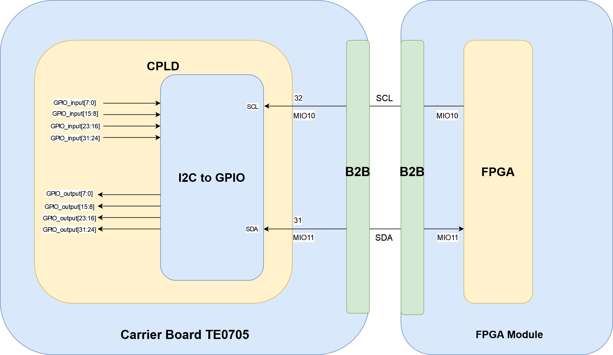
I2C bus is connected to MIO10 ( SCL signal) and MIO11 (SDA signal). MIO10 to MIO15 are direct connection between CPLD of TE0705 and FPGA on the module through B2B connector. If in FPGA design exists no i2c interface for MIO10 and MIO11, this block will be unused. More information about MIO10 to MIO15 are shown in the following table for whole Trenz Electronic 4x5 modules and TE0705 carrier board:
| B2B Pin | B2B JB1-96 | B2B JB1-94 | B2B JB1-100 | B2B JB1-98 | B2B JB1-91 | B2B JB1-86 | |
|---|---|---|---|---|---|---|---|
| Carrier board | Label / Firmware function | Label / Firmware function | Label / Firmware function | Label / Firmware function | Label / Firmware function | Label / Firmware function | Description |
| TE0705 | MIO10 / I2C-SCL | MIO11 / I2C-SDA | MIO12 / GPIO | MIO13 / GPIO | MIO14 / UART0-RX | MIO15 / USRT0-TX | MIO10 and MIO11 are used in CPLD firmware as I2C SCL and SDA respectively. |
| B2B Pin | B2B JM1-95 | B2B JM1-93 | B2B JM1-99 | B2B JM1-97 | B2B JM1-92 | B2B JM1-85 | |
| Module | Label / Chip pin | Label / Chip pin | Label / Chip pin | Label / Chip pin | Label / Chip pin | Label / Chip pin | Description |
| TEM0007 | I2C_CON_SCL / A3 | I2C_CON_SDA / E3 | UART_CON_TX / C2 | USRT_CON_RX / D3 | UART_RX / H2 | UART_TX / H5 | MIO10 and MIO11 are already set in test_design of TEM0007 as SCL and SDA respectively. |
| TE0710 | B14_IO2 / R10 | B14_IO6 / L18 | B14_IO7 / T11 | B14_IO3 / M18 | B16_IO4 / A8 | B16_IO0 / B8 | By using an external IIC IP core B14_IO2 and B14_IO6 can be used as I2C SCL and SDA respectively. |
| TE0711 | B14_IO2 / M13 | B14_IO6 / L18 | B14_IO7 / R16 | B14_IO3 / M18 | B14_IO4 / N17 | B14_IO0 / R10 | By using an external IIC IP core B14_IO2 and B14_IO6 can be used as I2C SCL and SDA respectively. |
| TE0712 | B14_L4_P / T21 | B14_L9_N / Y22 | B14_L24_N / R17 | B14_L4_N / U21 | B14_L24_P / P16 | B14_L18_N / U18 | By using an external IIC IP core B14_L4_P and B14_L9_N can be used as I2C SCL and SDA respectively. |
| TE0713 | B14_L4_P / T21 | B14_L9_N / Y22 | B14_L24_N / R19 | B14_L4_N / U21 | B14_L24_P / P19 | B14_L18_N / U18 | By using an external IIC IP core B14_L4_P and B14_L9_N can be used as I2C SCL and SDA respectively. |
| TE0741 | MIO10 / B14_L22 | MIO11 / B14_K21 | MIO12 / B14_H23 | MIO13 / B14_K22 | MIO14 / B14_J21 | MIO15 / B14_G24 | By using an external IIC IP core B14_L22 and B14_K21 can be used as I2C SCL and SDA respectively. |
| TE0841 | B65_SCL / Y19 | B65_SDA / AA19 | B65_L3_N / AF23 | B65_L3_P / AF22 | B65_L2_N / AH24 | B65_L4_N / AG24 | By using an external IIC IP core B65_SCL and B65_SDA can be used as I2C SCL and SDA respectively. |
| TE0715 | MIO10 / G16 | MIO11 / B19 | MIO12 / C18 | MIO13 / A17 | MIO14 / B17 | MIO15 / E17 | MIO10 and MIO11 can be set as SCL and SDA for I2C0 of TE0715 respectively. |
| TE0720 | MIO10 / G7 | MIO11 / B4 | MIO12 / C5 | MIO13 / A6 | MIO14 / B6 | MIO15 / E6 | MIO10 and MIO11 are already set as as SCL and SDA for I2C0 in test_design of TE0720 respectively. |
| TE0820 | MIO26 / L15 | MIO27 / J15 | MIO28 / K15 | MIO29 / G16 | MIO30 / F16 | MIO31 / H16 | MIO26 and MIO27 can be set only for I2C0 of FPGA and this bus is already used for another components same as EEPROM and PLL chip. If MIO10 and MIO11 are used as I2C bus for data communication with CPLD, then there are no access to PLL and EEPROM chip. |
| TE0821 | MIO26 / L15 | MIO27 / J15 | MIO28 / K15 | MIO29 / G16 | MIO30 / F16 | MIO31 / H16 | MIO26 and MIO27 can be set only for I2C0 of FPGA and this bus is already used for another components same as EEPROM and PLL chip. If MIO10 and MIO11 are used as I2C bus for data communication with CPLD, then there are no access to PLL and EEPROM chip. |
| TE0823 | MIO26 / L15 | MIO27 / J15 | MIO28 / K15 | MIO29 / G16 | MIO30 / F16 | MIO31 / H16 | MIO26 and MIO27 can be set only for I2C0 of FPGA and this bus is already used for another components same as EEPROM and PLL chip. If MIO10 and MIO11 are used as I2C bus for data communication with CPLD, then there are no access to PLL and EEPROM chip. |
There are more additional connections between CPLD and FPGA on the module , that are listed in the following table:
| CPLD Pin | Carrier board B2B Pin | Module B2B Pin | In firmware used as | Description |
|---|---|---|---|---|
| X6 | B2B JB1-84 | B2B JM1-83 | No specific function. It can only be read by GPIO_input. | It can be read via i2c to GPIO. ( GPIO_input(31) ) |
| Y0 | B2B JB2-76 | B2B JM2-75 | No specific function. It can only be read by GPIO_input. | It can be read via i2c to GPIO. ( GPIO_input(24) ) |
| Y1 | B2B JB2-78 | B2B JM2-77 | No specific function. It can only be read by GPIO_input. | It can be read via i2c to GPIO. ( GPIO_input(25) ) |
| Y2 | B2B JB2-82 | B2B JM2-81 | No specific function. It can only be read by GPIO_input. | It can be read via i2c to GPIO. ( GPIO_input(26) ) |
| Y3 | B2B JB2-84 | B2B JM2-83 | No specific function. It can only be read by GPIO_input. | It can be read via i2c to GPIO. ( GPIO_input(27) ) |
| Y4 | B2B JB2-86 | B2B JM2-85 | No specific function. It can only be read by GPIO_input. | It can be read via i2c to GPIO. ( GPIO_input(28) ) |
| Y5 | B2B JB2-88 | B2B JM2-87 | No specific function. It can only be read by GPIO_input. | It can be read via i2c to GPIO. ( GPIO_input(29) ) |
| Y6 | B2B JB2-90 | B2B JM2-89 | No specific function. It can only be read by GPIO_input. | It can be read via i2c to GPIO. ( GPIO_input(30) ) |
It is depends on the module , which bank and pin of FPGA is connected to the module B2B pins that are written in this table.
UART
| Pin | CPLD Pin | Connected to | Module UART Signal | Description |
|---|---|---|---|---|
| MIO14 | 40 | B2B JB1-91 | UART0-RX | In firmware MIO14 <= BDBUS0 |
| MIO15 | 30 | B2B JB1-86 | UART0-TX | In firmware BDBUS1 <= MIO15 |
NOSEQ
NOSEQ is used as TMS signal of JTAG port to program CPLD of TE0715 module. NOSEQ can be used as GPIO pin by user too. It can be controlled differentially for PCB REV03 and REV04 as in the following table is shown:
| NOSEQ | Condition for PCB REV04 or later | Condition for PCB REV03 | Related command in linux | Description |
|---|---|---|---|---|
| '0' | USR1 = OFF and USR0 = OFF | GPIO_output [15:8] = 0x01 , if access to TE0715 is programmed on the carrier board CPLD and CM1(S3-1)= OFF or CM0(S3-2)= OFF GPIO_output [15:8] = 0x01 , if no access to TE0715 CPLD is programmed on the carrier board CPLD , it is not dependent on CM0(S3-2) and CM1(S3-1). | i2cset -y 0 0x30 0x01 0x01 | If module has no i2c interface for MIO10 and MIO11 pins in vivado and linux design , this option for PCB REV03 does not work. |
| '1' | USR1 = ON and USR0 = OFF | GPIO_output [15:8] = 0x00 , if access to TE0715 is programmed on the carrier board CPLD and CM1(S3-1)= OFF or CM0(S3-2)= OFF GPIO_output [15:8] = 0x00 , if no access to TE0715 CPLD is programmed on the carrier board CPLD, it is not dependent on CM0(S3-2) and CM1(S3-1). | i2cset -y 0 0x30 0x01 0x00 | If module has no i2c interface for MIO10 and MIO11 pins in vivado and linux design , this option for PCB REV03 does not work. |
PGOOD
PGOOD pin is used as TDO JTAG signal to program CPLD of TE0715 module. PGOOD pin is used to select boot mode for SoC modules too. After booting user can use PGOOD as GPIO pin. PGOOD can be set or reset differentially for PCB REV04 and REV03 as shown:
| PGOOD | Condition for PCB REV04 or later | Condition for PCB REV03 | Related command in linux | Description |
|---|---|---|---|---|
| '0' | USR2 = OFF and USR0 = OFF | GPIO_output [23:16] = 0x01 , if access to TE0715 is programmed on the carrier board CPLD and CM1(S3-1)= OFF or CM0(S3-2)= OFF GPIO_output [23:16] = 0x01 , if no access to TE0715 CPLD is programmed on the carrier board CPLD, it is not dependent on CM0(S3-2) and CM1(S3-1). | i2cset -y 0 0x30 0x02 0x01 | If module has no i2c interface for MIO10 and MIO11 pins in vivado and linux design , this option for PCB REV03 does not work. |
| '1' | USR2 = ON and USR0 = OFF | GPIO_output [23:16] = 0x00 , if access to TE0715 is programmed on the carrier board CPLD and CM1(S3-1)= OFF or CM0(S3-2)= OFF GPIO_output [23:16] = 0x00 , if no access to TE0715 CPLD is programmed on the carrier board CPLD, it is not dependent on CM0(S3-2) and CM1(S3-1). | i2cset -y 0 0x30 0x02 0x00 | If module has no i2c interface for MIO10 and MIO11 pins in vivado and linux design , this option for PCB REV03 does not work. |
On-board LEDs
LED glows depending on various signals in firmware or pins of CPLD. Additionally to test I2C to GPIO output registers S1 push button can be used to display GPIO_output[7:0] register on LEDs. If S1 is pushed, ULED1 to ULED7 display GPIO_output[7:0] register. PHY_LED1/PHY_LED1_A and PHY_LED2/PHY_LED2_A are RJ45 connector right LED and RJ45 connector left LED respectively. These LEDs are using to display states of PGOOD, NOSEQ and EN_FMC signals.
| RJ45 Connector LED | Designator | LED Status | Condition | Description |
|---|---|---|---|---|
PHY_LED1 (Green LED Anode, Yellow LED Cathode) , PHY_LED1_A(Green LED Cathode, Yellow LED Anode) | J14C (Right LED) | OFF | PGOOD = '0', NOSEQ = '0' | |
| ON Yellow | PGOOD = '0', NOSEQ = '1' | |||
| ON Green | PGOOD = '1', NOSEQ = '0' | |||
| Blinky | PGOOD = '1', NOSEQ = '1' | |||
PHY_LED2 (Green LED Cathode , Yellow LED Anode) , PHY_LED2_A(Green LED Anode, Yellow LED Cathode) | J14B (Left LED) | ON Green | EN_FMC = '1' | Power Ok signal of EN5335QI PowerSoC is high. FMC_VADJ voltage is ok. |
| Blinky | EN_FMC = '0' | Power Ok signal of EN5335QI PowerSoC is low. FMC_VADJ voltage is faulty. |
| LED | Designator | Connected to Port / Signal | Condition | Connected to Port / Signal | Condition | Description |
|---|---|---|---|---|---|---|
| ULED1 | D6 | GPIO_output(0) | S1 = '0' (S1 push button is pushed) | mode0 | S1 = '1' (S1 is not pushed) | mode0 = '1' , If CM1(S3-1)= OFF and CM0(S3-2)= OFF FMC_VADJ = 1.8V |
| ULED2 | D7 | GPIO_output(1) | S1 = '0' (S1 push button is pushed) | mode1 | S1 = '1' (S1 is not pushed) | mode1 = '1' , If CM1(S3-1)= ON and CM0(S3-2)= OFF FMC_VADJ = 2.5V |
| ULED3 | D8 | GPIO_output(2) | S1 = '0' (S1 push button is pushed) | mode2 | S1 = '1' (S1 is not pushed) | mode2 = '1' , If CM1(S3-1)= OFF and CM0(S3-2)= ON FMC_VADJ = 3.3V |
| ULED4 | D9 | GPIO_output(3) | S1 = '0' (S1 push button is pushed) | mode3 | S1 = '1' (S1 is not pushed) | mode3 = '1' , If CM1(S3-1)= ON and CM0(S3-2)= ON FMC_VADJ = 1.8V |
| ULED5 | D4 | GPIO_output(4) | S1 = '0' (S1 push button is pushed) | S2 button (Reset) | S1 = '1' (S1 is not pushed) | If LED is ON --> S2 Reset push button is pushed. |
| ULED6 | D15 | GPIO_output(5) | S1 = '0' (S1 push button is pushed) | SD_DETECT | S1 = '1' (S1 is not pushed) | If LED is ON --> MODE = '1' (QSPI boot mode) else MODE = '0' (SD card boot mode) |
| ULED7 | D14 | GPIO_output(6) | S1 = '0' (S1 push button is pushed) | Module UART0-RX | S1 = '1' (S1 is not pushed) | |
| ULED8 | D5 | GPIO_output(7) | S1 = '0' (S1 push button is pushed) | Module UART0-TX | S1 = '1' (S1 is not pushed) |
I2C to GPIO registers access methods
I2C to GPIO subsystem has 4 output and 4 input 8 bit registers. These registers can be written or read in linux or FSBL code as shown in the following tables:
| GPIO input registers | Address | Read Command in Linux | Read Command in FSBL | Description |
|---|---|---|---|---|
| GPIO_input[7:0] | 0x00 | i2cget -y 0 0x30 0x00 | iic_read8(0x30,0x00,&data) | 0x30 is device address. ( I2C to GPIO address). |
| GPIO_input[15:8] | 0x01 | i2cget -y 0 0x30 0x01 | iic_read8(0x30,0x01,&data) | 0x30 is device address. ( I2C to GPIO address). |
| GPIO_input[23:16] | 0x02 | i2cget -y 0 0x30 0x02 | iic_read8(0x30,0x02,&data) | 0x30 is device address. ( I2C to GPIO address). |
| GPIO_input[31:24] | 0x03 | i2cget -y 0 0x30 0x03 | iic_read8(0x30,0x03,&data) | 0x30 is device address. ( I2C to GPIO address). |
| GPIO output registers | Address | Write Command in Linux | Write Command in FSBL | Description |
|---|---|---|---|---|
| GPIO_output[7:0] | 0x00 | i2cset -y 0 0x30 0x00 <data> | iic_write8(0x30,0x00,data) | 0x30 is device address. ( I2C to GPIO address). 0x00 is register address. |
| GPIO_output[15:8] | 0x01 | i2cset -y 0 0x30 0x01 <data> | iic_write8(0x30,0x01,data) | 0x30 is device address. ( I2C to GPIO address). 0x01 is register address. |
| GPIO_output[23:16] | 0x02 | i2cset -y 0 0x30 0x02 <data> | iic_write8(0x30,0x02,data) | 0x30 is device address. ( I2C to GPIO address). 0x02 is register address. |
| GPIO_output[31:24] | 0x03 | i2cset -y 0 0x30 0x03 <data> | iic_write8(0x30,0x03,data) | 0x30 is device address. ( I2C to GPIO address). 0x03 is register address. |
I2C to GPIO registers
| GPIO_input bit | Port/Signal | Description |
|---|---|---|
| 0 | VID0 | EN5335QI Power SoC Voltage Select Line 0 |
| 1 | VID1 | EN5335QI Power SoC Voltage Select Line 1 |
| 2 | VID2 | EN5335QI Power SoC Voltage Select Line 2 |
| 3 | USB_OC | USB Over Current |
| 4 | USR0 | DIP Switch S4-A |
| 5 | USR1 | DIP Switch S4-B |
| 6 | USR2 | DIP Switch S4-C |
| 7 | USR3 | DIP Switch S4-D |
| GPIO input bit | Port/Signal | Description |
|---|---|---|
| 8 | CM0(S3-2) | DIP Switch S3-B |
| 9 | CM1(S3-1) | DIP Switch S3-A |
| 10 | MIO10 | I2C-SCL |
| 11 | MIO11 | I2C-SDA |
| 12 | MIO12 | |
| 13 | MIO13 | |
| 14 | MIO14 | UART0-RX |
| 15 | MIO15 | UART0-TX |
| GPIO input bit | Port/Signal | Description |
|---|---|---|
| 16 | NOSEQ | |
| 17 | PGOOD | |
| 18 | SD_WP | |
| 19 | SD_DETECT | |
| 20 | S1 | User Button |
| 21 | POK_FMC | FMC VADJ Power Good |
| 22 | ACBUS4 | |
| 23 | ACBUS5 |
| GPIO input bit | Port/Signal | Description |
|---|---|---|
| 24 | Y0 | |
| 25 | Y1 | |
| 26 | Y2 | |
| 27 | Y3 | |
| 28 | Y4 | |
| 29 | Y5 | |
| 30 | Y6 | |
| 31 | X6 |
| GPIO output register | Port / Signal | Condition | Description |
|---|---|---|---|
| GPIO_output [7:0] | ULEDs | S1 (User push button) = ON (pushed) | To test GPIO_output it is helpful to check the sent data via i2c to GPIO on the ULEDs. |
| GPIO_output [15:8] | vir_usr1 | GPIO_output[15:8] = 0x00 → vir_usr1 = '0' GPIO_output[15:8] = 0x01 → vir_usr1 = '1' | This register is used to control NOSEQ pin for PCB REV03. If no access to TE0715 CPLD or access to TE0715 CPLD jed file is programmed on the CPLD of carrier board and CM0(S3-2) and CM1(S3-1) are OFF: |
| GPIO_output [23:16] | vir_usr2 | GPIO_output[23:16] = 0x00 → vir_usr2 = '0' | This register is used to control PGOOD pin for PCB REV03. If no access to TE0715 CPLD or access to TE0715 CPLD jed file is programmed on the CPLD of carrier board and CM0(S3-2) and CM1(S3-1) are OFF: vir_usr2 = '1' → PGOOD= '0' * |
| GPIO_output [31:24] | ---- | ----- | ---- |
*Note: This is only valid for PCB REV03. For PCB REV04 vir_usr1,vir_usr2 and vir_usr3 are not be used. For PCB REV04 PGOOD and NOSEQ can be controlled via USR2 and USR1 dip switches respectively.
Appx. A: Change History
Revision Changes
REV02 to REV03
JTAG timing correction
Renaming ports according to the schematic REV04
RGPIO is removed.
I2C to GPIO sub system is added for communication between FPGA on the module and CPLD on the carrier board. (MIO10 --> SCL , MIO11 --> SDA)
Access to CPLD chip of TE0715 either via USR0 Dip switch for PCB REV04 or via CM0 and CM1 for PCB REV03 revisions
In PCB REV04 USR0 is used to access to TE0715 CPLD
In PCB REV04 USR1 is used to change NOSEQ signal, if no access to TE0715 CPLD is active (USR0 = OFF)
In PCB REV04 USR2 is used to change PGOOD, if no access to TE0715 CPLD is active (USR0 = OFF)
In PCB REV04 USR3 is used to change JTAGMODE signal of CPLD of module. USR3 = OFF --> Access to FPGA , USR3 = ON --> Access to CPLD of module
In PCB REV03 CM0 and CM1 dip switches are used to access to CPLD of TE0715 or other modules.
Displaying PGOOD and NOSEQ signal states on PHY_LED1/PHY_LED1_A
Displaying state of POK_FMC ( power ok signal of EN5335QI PowerSoC) on PHY_LED2/PHY_LED2_A
REV01 to REV02
- Power Management
- VADJ is switchable by S3 dip switches
- Reset Management
- only little changes
- RGPIO Interface to FPGA
- RGPIO support
- LED
- new Order and accessible by RGPIO
- Module CPLD access is possible know
Document Change History
To get content of older revision got to "Change History" of this page and select older document revision number.
|
| Date | Document Revision | CPLD Firmware Revision | Supported PCB Revision | Authors | Description |
|---|---|---|---|---|---|
| REV03 | REV03, REV04 |
| |||
2017-06-08 | v.34 | REV02 | REV03,REV04 | John Hartfiel | document style update |
| 2016-11-17 | v.27 | REV02 | REV03, REV04 | John Hartfiel | Revision 02 finished |
| 2016-11-04 | v.1 | --- | Initial release | ||
| All |
Appx. B: Legal Notices
|
<style>
.wiki-content .columnLayout .cell.aside {
width: 20%;
}</style>
|
|