Module: TRM Name always "TE Series Name" +TRM Example: "TE0728 TRM"
Carrier: TRM Name usually "TEB Series Name" +TRM Example: "TEB0728 TRM"
<!-- tables have all same width (web max 1200px and pdf full page(640px), flexible width or fix width on menu for single column can be used as before) -->
<style>
.wrapped{
  width: 100% !important;
  max-width: 1200px !important;
 }
</style>
Important General Note:
If some section is configurable and depends on Firmware, please refer to the addition page (for example CPLD). If not available, add note, that this part is configurable
Designate all graphics and pictures with a number and a description, Use "Scroll Title" macro
Use "Scroll Title" macro for pictures and table labels. Figure number must be set manually at the moment (automatically enumeration is planned by scrollPDF)
Figure template:
Create DrawIO object here: Attention if you copy from other page, objects are only linked.
image link to the generate DrawIO PNG file of this page. This is a workaround until scroll pdf export bug is fixed
Table template:
Layout macro can be use for landscape of large tables
Example
Comment
1
2
The anchors of the Scroll Title should be named consistant across TRMs. A incomplete list of examples is given below
<type>_<main section>_<name>
type: Figure, Table
main section:
"OV" for Overview
"SIP" for Signal Interfaces and Pins,
"OBP" for On board Peripherals,
"PWR" for Power and Power-On Sequence,
"B2B" for Board to Board Connector,
"TS" for Technical Specification
"VCP" for Variants Currently in Production
"RH" for Revision History
name: custom, some fix names, see below
Fix names:
"Figure_OV_BD" for Block Diagram
"Figure_OV_MC" for Main Components
"Table_OV_IDS" for Initial Delivery State
"Table_PWR_PC" for Power Consumption
"Figure_PWR_PD" for Power Distribution
"Figure_PWR_PS" for Power Sequence
"Figure_PWR_PM" for Power Monitoring
"Table_PWR_PR" for Power Rails
"Table_PWR_BV" for Bank Voltages
"Table_TS_AMR" for Absolute_Maximum_Ratings
"Table_TS_ROC" for Recommended_Operating_Conditions
"Figure_TS_PD" for Physical_Dimensions
"Table_VCP_SO" for TE_Shop_Overview
"Table_RH_HRH" for Hardware_Revision_History
"Figure_RH_HRN" for Hardware_Revision_Number
"Table_RH_DCH" for Document_Change_History
Use Anchor in the document: add link macro and add "#<anchorname>
Refer to Anchror from external : <page url>#<pagename without space characters>-<anchorname>
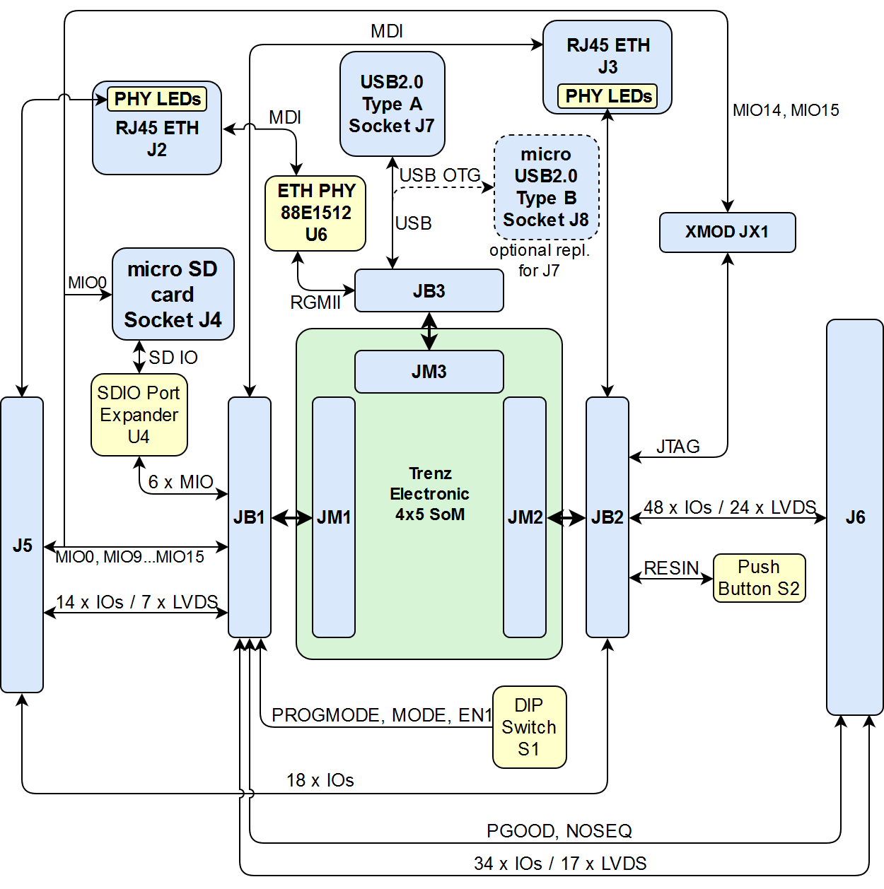
The Trenz Electronic TE0706 Carrier Board provides functionalities for testing, evaluation and development purposes of company's 4 x 5 cm SoMs. The Carrier Board is equipped with various components and connectors for different configuration setups and needs. The interfaces of the SoM's functional units and PL I/O-banks are connected via board-to-board connectors to the Carrier Board's components and connectors for easy user access.
See "4 x 5 SoM Carriers" page for more information about supported 4 x 5 cm SoMs.
Refer to http://trenz.org/te0706-info for the current online version of this manual and other available documentation.
VG96 connector (mounting holes and solder pads, J6) and 50-pin IDC male connector socket (J5) for access to PL I/O-bank pins
USB2.0 type A connector, or optionally Micro USB 2.0 connector
1 x RJ45 GbE MagJack (J3), connected via MDI to B2B connector JB1
1 x Marvell Alaska 88E1512 GbE PHY, providing Ethernet interface in conjunction with RJ45 GbE MagJack (J2)
4 A High-Efficiency Power SoC DC-DC Step-Down Converter (Enpirion EN6347) for 3.3V power supply
XMOD JTAG- / UART-header JX1
Micro SD card socket
SDIO port expander with voltage-level translation and jumper (J13) for selection of SDIO voltage on SoM side
DIP-switches S1 to set SoM's control signals
1 x user-push button (S2), by default configured as system reset button
3 x VCCIO selection jumper J10, J11 and J12 to set SoM's PL I/O-bank voltages
5V power supply barrel jack
Additional assembly options are available for cost or performance optimization upon request.
Block Diagram
add drawIO object here.
For more information regarding how to draw a diagram, Please refer to "Diagram Drawing Guidline" .
Main Components
Notes :
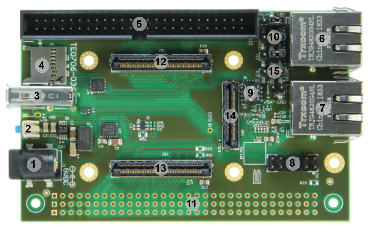
Picture of the PCB (top and bottom side) with labels of important components
Add List below
For more information regarding how to add board photoes, Please refer to "Diagram Drawing Guidline" .
5V power connector jack, J1
Reset switch, S2
USB2.0 type A receptacle, J7
Micro SD card socket with Card Detect, J4
50 pin IDC male connector, J5
1000Base-T Gigabit RJ45 Ethernet MagJack, J3
1000Base-T Gigabit RJ45 Ethernet MagJack, J2
XMOD JTAG- / UART-header, JX1
User DIP-switch, S1
VCCIO selection jumper block, J10 - J12
External connector (VG96) placeholder, J6
Samtec Razor Beam™ LSHM-150 B2B connector, JB1
Samtec Razor Beam™ LSHM-150 B2B connector, JB2
Samtec Razor Beam™ LSHM-130 B2B connector, JB3
SoM SDIO voltage selection jumper, J13
Initial Delivery State
Notes :
Only components like EEPROM, QSPI flash and DDR3 can be initialized by default at manufacture.
If there is no components which might have initial data ( possible on carrier) you must keep the table empty
There is no hardware component to be programmed on the carrier.
Storage device name
Content
Notes
---
---
---
Board is shipped in following configuration:
VCCIO voltage selection jumpers are all set to 1.8 V.
S2 switch configured as reset button.
Different delivery configurations are available upon request.
Configuration Signals
Overview of Boot Mode, Reset, Enables.
Signal
Designator
B2B
State
Description
Note
MODE
S1-3
JB1-31
ON
Drive SoM SC CPLD pin 'MODE' low.
Usually SD-Boot
OFF
Leave SoM SC CPLD pin 'MODE' open.
Usually QSPI-Boot
EN1
S1-4
JB1-27
ON
Drive SoM SC CPLD pin 'EN1' low.
Usually used to enable/disable FPGA core-voltage supply. (Depends also on SoM's SC CPLD firmware).
Note: Power-on sequence will be intermitted if S1-4 is set to OFF and if functionality is supported by SoM.
OFF
Drive SoM SC CPLD pin 'EN1' high.
There is a user push button which is used for RESET signal.
Signal
Designator
B2B
Note
RESIN
S2
JB2-17
Aktive Low
Signals, Interfaces and Pins
Notes :
For carrier or stand-alone boards use subsection for every connector type (add designator on description, not on the subsection title), for example:
SD
USB
ETH
FMC
...
For modules which needs carrier use only classes and refer to B2B connector if more than one is used, for example
JTAG
UART
I2C
MGT
...
Board to Board (B2B) I/Os
With the TE0706 Carrier Board's Board-to-Board Connectors (B2B) the MIO- and PL I/O-bank's pins and further interfaces of the mounted SoM can be accessed. A large quantity of these I/Os are also usable as LVDS-pairs. The connectors provide also VCCIO voltages to operate the I/Os properly.
Following table gives a summary of the available I/Os, interfaces and LVDS-pairs of the B2B connectors JB1, JB2 and JB3:
B2B Connector
Interfaces
Count of I/Os
Notes
JB1
User I/O
48 single ended or 24 differential
-
8 single ended
MIO with Zynq Modules
GbE MagJack J3 MDI
8
-
SD IO
6
-
SoM control signals
5
EN1, PGOOD, MODE, NOSEQ, PRPGMODE
JB3
GbE PHY U6 RGMII
18
-
USB2.0 (OTG, device and host mode)
5
-
JB2
User I/O
18 single ended
-
48 single ended or 24 differential
-
JTAG
4
-
SoM control signals
1
RESIN
GbE MagJack J3 LEDs
2
-
On-board Connector
The TE0706 Carrier Board has a 50-pin IDC male connector J5 and soldering pads as place-holder to mount a VG96 connectors J6 to get access the PL I/O-bank's pins and further interfaces of the mounted SoM. With these connectors, SoM's PL-I/Os are available to the user, a large quantity of these I/Os are also usable as differential pairs.
Following table gives a summary of the pin-assignment, available interfaces and functional I/Os of the connectors J5 and J6:
On-board Connector
Control Signals and Interfaces
Count of I/Os
Notes
J5
User I/O
18 single ended
-
14 single ended or 7 differential
-
MIO
8
-
GbE MagJack J2 LEDs
2
-
J6
User I/O
82 single ended or 41 differential
-
SoM control signals
2
'PGOOD', 'NOSEQ'
JTAG/UART Interface Base
JTAG/UART access to the TE0706 carrier is available through XMOD header JX1, which has a 'XMOD FTDI JTAG Adapter'-compatible pin-assignment. This header provides also a UART interface, usually established by MIO-pins of the PS-bank of the mounted SoM's Zynq device. XMOD USB2.0 to JTAG/UART adapter TE0790 is provided by Trenz Electronic. More information is available here. Devices of the mounted SoM can be programed via USB2.0 interface.
XMOD Designator
Designator
B2B Pin
XMOD Header JX1
Note
3.3V
-
-
JX1-5
NC
A
MIO15
JB1-86
JX1-3
UART Txd - (transmit line)
B
MIO14
JB1-91
JX1-7
UART Rxd - (receive line)
C
TCK_B
JB2-100
JX1-4
JTAG-TCK
D
TDO_B
JB2-98
JX1-8
JTAG-TDO
E
XMOD_E
-
-
NC
F
TDI_B
JB2-96
JX1-10
JTAG-TDI
G
XMOD_G
-
-
NC
H
TMS_B
JB2-94
JX1-12
JTAG-TMS
VIO
VCCJTAG
JB2-92
JX1-6
VIO is connected to 3.3V which is supplied by carrier
When using XMOD FTDI JTAG Adapter TE0790, the adapter-board's VIO will be sourced by the mounted SoM's 'VCCJTAG' (pin JB2-92). Set the DIP-switch with the setting:
XMOD DIP-switches
Position
Switch 1
ON
Switch 2
OFF
Switch 3
OFF
Switch 4
ON
Use AMD compatible TE0790 adapter board (designation TE-0790-xx with out 'L') to program the AMD Zynq devices.
The TE0790 adapter board's CPLD have to be configured with the Standard variant of the firmware. Refer to the TE0790 Resources Site for further information and firmware download.
SD Card Socket
The SD Socket is routed to the on-board Texas Instruments TXS02612 SDIO port expander U4. This IC provides a necessary VDD/VCCIO translation between the MicroSD Card socket J4 (3.3V) and the SoM's Zynq device MIO-bank (1.8V/3.3V depending on Module, compare jumper J13 ):
SD IO Signal Schematic Name
Connected to
Note
eSD_DAT0
U4-18
SD IO data
eSD_DAT1
U4-16
SD IO data
eSD_DAT2
U4-23
SD IO data
eSD_DAT3
U4-22
SD IO data
eSD_CLK
U4-19
SD IO clock
eSD_CMD
U4-20
SD IO command
MIO0
J5-29
Card Detect signal
USB2.0 connector
TE0706-03 board has one physical USB2.0 type A socket J7, the differential data signals of the USB2.0 socket are routed to the B2B connector JB3, where they can be accessed by the corresponding USB2.0 PHY transceiver of the mounted SoM.
There is also the option to equip the board with a Micro USB 2.0 type B (receptacle) socket (J8) to the board as alternative fitting option. With this fitting option (Micro USB2.0 type B), the USB2.0 interface can also be used for Device mode, OTG and Host Modes.
For USB2.0 Host mode, the Carrier Board is additionally equipped with a power distribution switch U5 to provide the USB2.0 interface with the USB supply voltage USB-VBUS with nominal value of 5V. OTG mode is not available with USB2.0 Type A socket.
Following table gives an overview of the USB2.0 connector signals:
USB2.0 Signal Schematic Name
B2B
Connected to (type A)
Connected to (optional replacement for type A J7)
Note
OTG-D_N
JB2-48
J7-2
J8-2
USB2.0 data
OTG-D_P
JB2-50
J7-3
J8-3
USB2.0 data
OTG-ID
JB2-52
NC
J8-4
Ground this pin for A-Device (host), left floating this pin for B-Device (peripheral).
VBUS_V_EN
JB2-54
U5-4
U5-4
Enable USB-VBUS.
USB-VBUS
JB2-56
J7-1
J8-1
USB supply voltage in Host mode.
RJ45 Gigabit Ethernet Connectors
The TE0706 Carrier Board is equipped with two Gigabit Ethernet ports. One of them (J2) is routed to Marvell Alaska 88E1512 Gigabit Ethernet PHY (U6). The GbE MegJack J2 has two integrated LEDs (both green), its signals are routed as MDI (Media Dependent Interface) to the GbE PHY. The MegJack J3 is connected via MDI directly to the B2B connector JB1. There is usually a corresponding Gigabit Ethernet PHY on 4 x 5 SoMs (e.g. TE0715 or TE0720), which can be used in conjunction with the baseboard MagJack J3.
MegJack J2
Signal
Connected to
J2-2
PHY2_MDI0_P
U6-28
J2-3
PHY2_MDI0_N
U6-27
J2-4
PHY2_MDI1_P
U6-24
J2-5
PHY2_MDI1_N
U6-23
J2-6
PHY2_MDI2_P
U6-22
J2-7
PHY2_MDI2_N
U6-21
J2-8
PHY2_MDI3_P
U6-18
J2-9
PHY2_MDI3_N
U6-17
J2 Green MegJack LED
PHY_LED0
U6-14
J2 Green MegJack LED
PHY_LED1
U6-13
MegJack J3
Signal
B2B
J3-2
PHY_MDI0_P
JB1-3
J3-3
PHY_MDI0_N
JB1-5
J3-4
PHY_MDI1_P
JB1-9
J3-5
PHY_MDI1_N
JB1-11
J3-6
PHY_MDI2_P
JB1-15
J3-7
PHY_MDI2_N
JB1-17
J3-8
PHY_MDI3_P
JB1-21
J3-9
PHY_MDI3_N
JB1-23
J3 Green MegJack LED
ETH_LED1
JB2-90
J3 Yellow MegJack LED
ETH_LED2
JB2-99
MIO Pins
you must fill the table below with group of MIOs which are connected to a specific components or peripherals, you do not have to specify pins in B2B, Just mention which B2B is connected to MIOs. The rest is clear in the Schematic.
Example:
MIO Pin
Connected to
B2B
Notes
MIO12..14
SPI_CS , SPI_DQ0... SPI_DQ3
SPI_SCK
J2
QSPI
Signal (MIO Pin)
Connected to
B2B
Notes
MIO0
micro SD-Card, J5-29
JB1-88
Card detect
MIO9
J5-30
JB1-92
MIO10
J5-28
JB1-96
I²C clock line
MIO11
J5-27
JB1-94
I²C data line
MIO12
J5-26
JB1-100
MIO13
J5-25
JB1-98
MIO14
XMOD, J5-32
JB1-91
UART
MIO15
XMOD, J5-31
JB1-86
6 x MIO
SD-Card
JB1
B2B positions see SDIO Port Expander. MIO positions depend on attached SoM.
On-board Peripherals
Notes :
add subsection for every component which is important for design, for example:
Two 100 Mbit Ethernet Transciever PHY
USB PHY
Programmable Clock Generator
Oscillators
eMMCs
RTC
FTDI
...
DIP-Switches
Buttons
LEDs
Notes :
In the on-board peripheral table "chip/Interface" must be linked to the corresponding chapter or subsection
Table below describes DIP-switch S1 settings for configuration of the mounted SoM:
Switch
Signal Name
ON
OFF
Notes
S1-1
-
-
-
Not connected.
S1-2
PROGMODE
JTAG enabled for programing mounted SoM's Zynq-SoC.
JTAG enabled for programing mounted SoM's SC-CPLD.
-
S1-3
MODE
Drive SoM SC CPLD pin 'MODE' low. (SD-Boot)
Leave SoM SC CPLD pin 'MODE' open. (QSPI-Boot)
Boot mode configuration, if supported by SoM. (Depends also on SoM's SC-CPLD firmware).
S1-4
EN1
Drive SoM SC CPLD pin 'EN1' low.
Drive SoM SC CPLD pin 'EN1' high.
Usually used to enable/disable FPGA core-voltage supply. (Depends also on SoM's SC CPLD firmware).
Note: Power-on sequence will be intermitted if S1-4 is set to OFF and if functionality is supported by SoM.
Note: Compared to the former revision 02 of this board, the DIP-switch is rotated by 180° due to routing issues.
VCC Selection Jumpers
Note: The corresponding PL I/O-bank supply-voltages of the 4 x 5 SoM to the selectable base-board voltages VCCIOA, VCCIOB and VCCIOC are depending on the mounted 4 x 5 SoM and varying in order of the used model.
Refer to the SoM's schematic for information about the specific pin assignments on module's B2B-connectors regarding the PL I/O-bank supply-voltages and to the 4 x 5 Module integration Guide for VCCIO voltage options.
The Carrier Board VCCIO for the PL I/O-banks of the mounted SoM are selectable by the jumpers J10, J11 and J12.
Following table describes how to configure the VCCIO of the SoM's PL I/O-banks with jumpers:
Supply Voltage by Jumper
Supply Voltage by 0-Ohm Resistor
Supply Connector Pin
Supplied Connector Pin
Voltage Level
1.8V
3.3V
1.8V
3.3V
VCCIOA
J10: 1-2, 3
J10: 1, 2-3
-
R20
J6-B32
JB1-10, JB1-12
VCCIOB
J11: 1-2, 3
J11: 1, 2-3
R29
R21
-
JB2-6
VCCIOC
J12: 1-2, 3
J12: 1, 2-3
R30
R22
J6-B1
JB2-8, JB2-10
Only one supply-source is allowed to configure the base-board supply-voltages, either by jumper, by 0-Ohm-resistor or by connector J6. If a supply-voltage is configured by 0-Ohm-resistor or connector J6, then the corresponding configuration-jumper has to be removed. There aren't 0-Ohm-resistors and supply-voltages by connector J6 allowed if the corresponding base-board supply-voltage is configured by jumper. Vice versa jumpers and 0-Ohm-resistors have to be removed if supplying corresponding base-board supply-voltage by connector J6.
Note: If supplying base-board supply-voltages by connector J6, the module's internal 3.3V voltage-level on pins 9 and 11 of B2B-connector JB2 has to be reached stable state.
Take care of the VCCO voltage ranges of the particular PL IO-banks (HR, HP) of the mounted SoM, otherwise damages may occur to the FPGA. Therefore, refer to the TRM of the mounted SoM to get the specific information of the voltage ranges.
It is recommended to set and measure the PL IO-bank supply-voltages before mounting of TE 4 x 5 module to avoid failures and damages to the functionality of the mounted SoM.
The SDIO voltage on the SoM side can be selected by jumper J13.
Supply Voltage by Jumper
Supplied Connector Pin
Voltage Level
1.8V
3.3V
SD_VCCA
J13: 1-2, 3
J13: 1, 2-3
U4-5
RTC Buffer Voltage Supply Header
The buffer voltage of the SoM's RTC can be supplied through the header J9 (VBAT-pin). Refer to the SoM's TRM for recommended voltage range and absolute maximum ratings.
Push Button
The Carrier Board's push button S2 is connected to the 'RESIN' signal, the function of the button is to trigger a reset of the mounted SoM by driving the reset-signal 'RESIN' to ground.
Gigabit Ethernet PHY
The TE0706 Carrier Board is equipped with a Marvell Alaska 88E1512 Gigabit Ethernet PHY (U6), which provides in conjunction with the Gigabit Ethernet MagJack J2 a 1000Base-T Ethernet (GbE) interface. The Ethernet PHY RGMII interface is connected to the B2B connector JB3, where they can be accessed by the mounted SoM's PS bank. The I/O Voltage is fixed at 1.8V. Reference clock input of the PHY is supplied from the on-board 25.000000 MHz oscillator (U7), the 125MHz output clock signal *CLK125' is connected to the B2B connector pin JB3-32.
PHY U6 pins
B2B-pin
Notes
ETH-MDC/ETH-MDIO
JB3-49, JB3-51
-
PHY_LED0
-
Connected to GbE MagJack J2 LED0 (green). Also connected to J5-24 (PHY_LED0_CON).
PHY_LED1
-
Connected to GbE MagJack J2 LED1 (green). Also connected to J5-23 (PHY_LED1_CON).
PHY_INT
JB3-33
-
CONFIG
JB3-60
-
CLK125
JB3-32
PHY Clock (125 MHz) output.
ETH-RST
JB3-53
-
RGMII
JB3-31 JB3-37 - JB-44 JB3-47 JB3-57 - JB-59
Reduced Gigabit Media Independent Interface. 12 pins.
ETH-RXCK is connected via 0Ohm to JB3-31 (R18)and JB3-58 (R19). Usage depends on Module and AMD IP restrictions In case of performance problems remove 0Ohm resistor from the unused Pin.
The TE0706 Carrier Board is equipped with a Texas Instruments TXS02612 SDIO Port Expander, which is needed for voltage translation due to different voltage levels of the Micro SD Card and the PS MIO-bank of the Zynq device of the mounted SoM. The Micro SD Card has 3.3V signal voltage level, but the PS MIO-bank on the AMD Zynq module has VCCIO of 1.8V or 3.3V depending on the attached module. This has to be selected by J13.
SD-Card Signal Schematic Name
SD-Card Connected to
Connected to
SD IO Signal Schematic Name
B2B
Note
eSD_DAT0
U4-18
U4-6
SD_DAT0
JB1-24
SD IO data
eSD_DAT1
U4-16
U4-7
SD_DAT1
JB1-22
SD IO data
eSD_DAT2
U4-23
U4-1
SD_DAT2
JB1-20
SD IO data
eSD_DAT3
U4-22
U4-3
SD_DAT3
JB1-18
SD IO data
eSD_CLK
U4-19
U4-9
SD_CLK
JB1-28
SD IO clock
eSD_CMD
U4-20
U4-4
SD_CMD
JB1-26
SD IO command
MIO0
-
-
-
JB1-88
Card Detect signal
Power and Power-On Sequence
In 'Power and Power-on Sequence' section there are three important digrams which must be drawn:
Power on-sequence
Power distribution
Voltage monitoring circuit
For more information regarding how to draw diagram, Please refer to "Diagram Drawing Guidline" .
Power Supply
Power supply with minimum current capability of 3A for system startup is recommended.
Power Consumption
The maximum power consumption of the Carrier Board depends mainly on the mounted SoM's FPGA design running on the Zynq device.
AMD provide a power estimator excel sheets to calculate power consumption. It's also possible to evaluate the power consumption of the developed design with Vivado. See also Trenz Electronic Wiki FAQ.
Power Input Pin
Typical Current
VIN
TBD*
VBAT
TBD*
* TBD - To Be Determined.
Power supply with minimum current capability of 3A for system startup is recommended.
To avoid any damage to the module, check for stabilized on-board voltages and VCCIOs before put voltages on PL I/O-banks and interfaces. All I/Os should be tri-stated during power-on sequence.
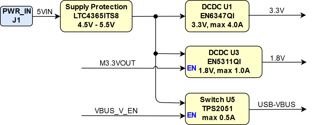
Power Distribution Dependencies
The Carrier Board needs one single power supply voltage with a nominal value of 5V. Following diagram shows the distribution of the input voltage '5VIN' to the on-board components on the mounted SoM:
Power Rails
The voltage direction of the power rails is directed at on-board connectors' view:
Module Connector (B2B) Designator
VCC / VCCIO
Direction
Pins
Notes
JB1
3.3V
Out
2, 4, 6, 14, 16
3.3V module supply voltage
VCCIOA
Out
10, 12
PL IO-bank VCCIO
M1.8VOUT
In
40
1.8V module output voltage
VBAT
Out
80
RTC buffer voltage
JB2
1.8V
Out
2, 4
1.8V module supply voltage
VCCIOB
Out
6
PL IO-bank VCCIO
VCCIOC
Out
8, 10
PL IO-bank VCCIO
M3.3VOUT
In
9, 11
3.3V module output voltage
VCCJTAG
In
92
3.3V JTAG VCCIO
JB3
USB-VBUS
Out
56
USB Host supply voltage
On-board Connector Designator
VCC / VCCIO
Direction
Pins
Notes
J5
3.3V
Out
6, 45
3.3V module supply voltage
M3.3VOUT
Out
5, 46
3.3V module output voltage
J6
VCCIOA
Out / In
B32
PL IO-bank VCCIO, depends on Jumper settings
VCCIOC
Out / In
B1
PL IO-bank VCCIO, depends on Jumper settings
M3.3VOUT
Out
C32
3.3V module output voltage
3.3V
Out
C31
3.3V module supply voltage
5VIN
Out
A1, A2
Carrier Board supply power
Jumper / Header Designator
VCC / VCCIO
Direction
Pins
Notes
J10
VCCIOA
In
2
-
1.8V
Out
1
-
M3.3VOUT
Out
3
-
J11
VCCIOB
In
2
-
1.8V
Out
1
-
M3.3VOUT
Out
3
-
J12
VCCIOC
In
2
-
1.8V
Out
1
-
M3.3VOUT
Out
3
-
Main Power Jack and Pins Designator
VCC / VCCIO
Direction
Pins
Notes
J1
5VIN
In
1
Power Jack 2.1mm 90° SMD
J9
VBAT
In
1
Attention: Pin 2 connected to ground. VBAT voltage connected on this pin cause short-circuit.
Peripheral Socket Designator
VCC / VCCIO
Direction
Pins
Notes
J7 / J8
USB-VBUS
In / Out
1
Direction depends on USB mode
J4
M3.3VOUT
Out
4
MikroSD Card socket VDD
XMOD Header Designator
VCC / VCCIO
Direction
Pins
Notes
JX1
3.3V
-
5
not connected
VIO
Out
6
connected to 'VCCJTAG' (pin JB2-92)
Board to Board Connectors
Technical Specifications
Absolute Maximum Ratings
Parameter
Min
Max
Units
Reference Document
5VIN supply voltage
-0.3
7
V
MP5010A, EN6347QI, EN5311QI data sheet
Storage temperature
-55
+85
°C
Marvell 88E1512 data sheet
Recommended Operating Conditions
Operating temperature range depends also on customer design and cooling solution. Please contact us for options.
Parameter
Min
Max
Units
Reference Document
5VIN supply voltage
4.75
5.25
V
USB2.0 specification concerning 'VBUS' voltage
Operating temperature
-40
+85
°C
-
The TE0706 Carrier Board itself is capable to be operated at industrial grade temperature range (-40 °C ..+85 °C).
Please check the operating temperature range of the mounted SoM, which determine the relevant operating temperature range of the overall system.
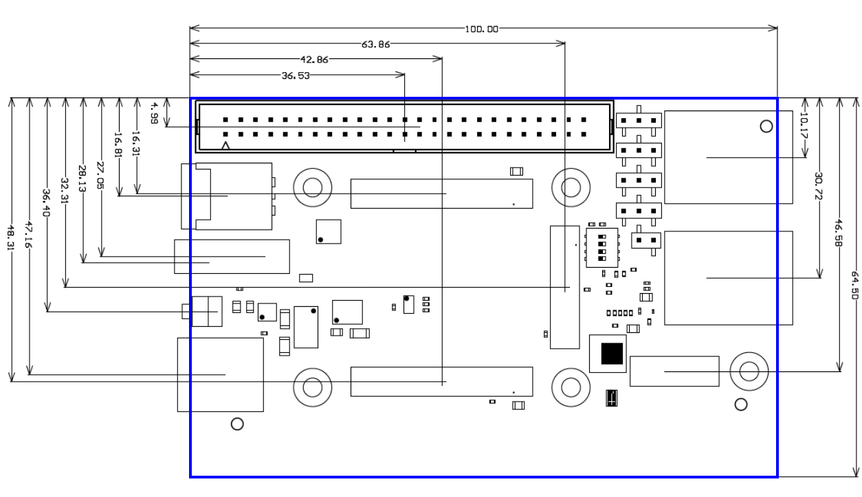
Physical Dimensions
Board size: PCB 100mm × 64.5mm. Notice that the USB type A socket on the left and the Ethernet RJ-45 jacks on the right are hanging slightly over the edge of the PCB making the total width of the longer side approximately 106mm. Please download the assembly diagram for exact numbers.
Mating height of the module with standard connectors: 8mm
PCB thickness: 1.65mm
Highest parts on the PCB are USB type A socket and the Ethernet RJ-45 jacks, approximately 15mm. Please download the step model for exact numbers.
In 'Physical Dimension' section, top and button view of module must be insterted, information regarding physical dimensions can be obtained through webpage for product in Shop.Trenz, (Download> Documents> Assembly part)for every SoM.
For Example: for Module TE0728, Physical Dimension information can be captured by snipping tools from the link below:
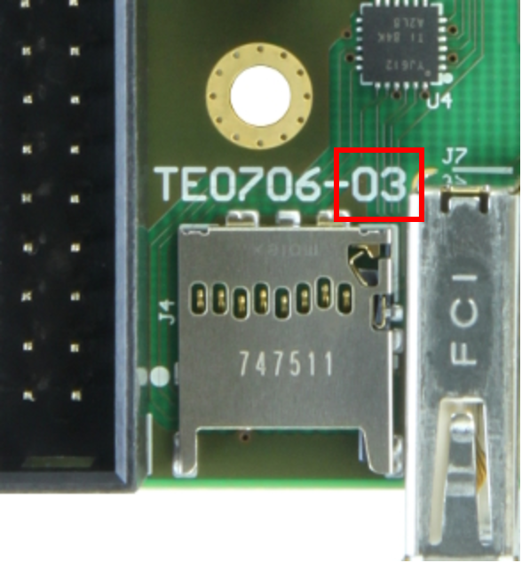
Hardware revision number can be found on the PCB board together with the module model number separated by the dash.
Document Change History
<!--
Generate new entry:
1.add new row below first
2.Copy "Page Information Macro(date)" Macro-Preview, Metadata Version number, Author Name and description to the empty row. Important Revision number must be the same as the Wiki document revision number
3.Update Metadata = "Page Information Macro (current-version)" Preview+1 and add Author and change description.
  -->