Table of Contents
Download PDF version of this document. |
Table of Contents |
Refer to "https://shop.trenz-electronic.de/de/Download/?path=Trenz_Electronic/TE0723/REV03/Documents" for downloadable version of this manual and additional technical documentation of the product. |
The Trenz Electronic TE0723-03 is a Arduino compatible FPGA module based on the Xilinx ZYNQ XC7Z010 SoC.
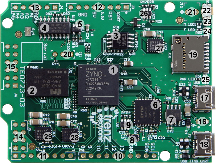
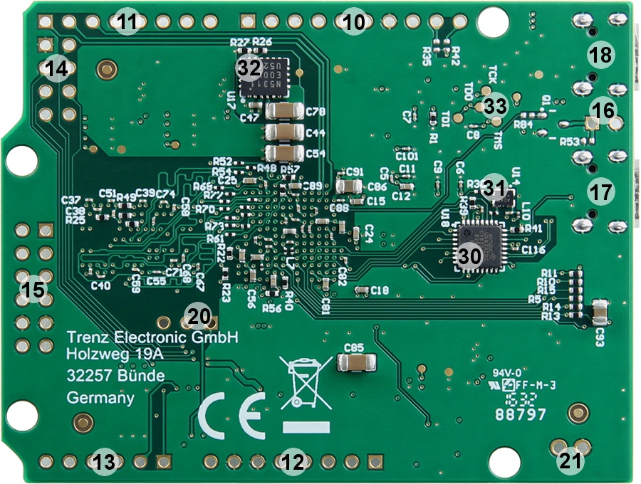
High-speed CMOS logic analog multiplexer/demultiplexer, U10
1A PowerSoC DC-DC converter (3.3 V), U20
Additional assembly options are available for cost or performance optimization upon request.
Storage device name | Content | Notes |
|---|---|---|
QSPI Flash | Empty |
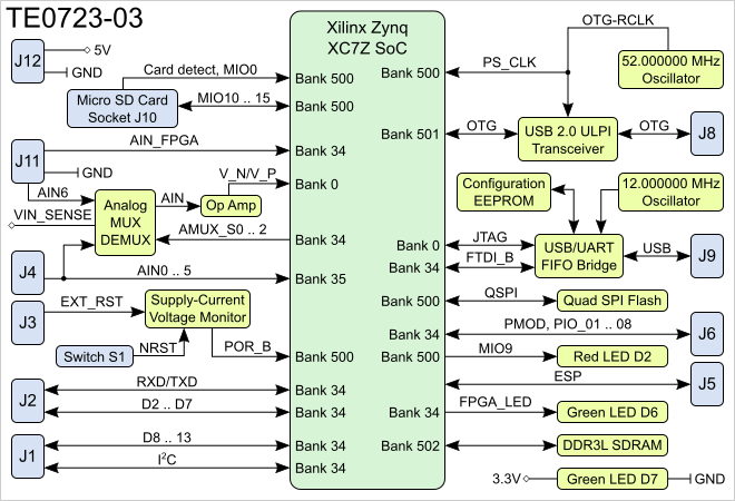
List of signals between PS/PL banks and external connectors:
| Bank | Type | Connector | I/O Signal Count | Voltage | Notes |
|---|---|---|---|---|---|
| 34 | HR | J1 | 6 | 3.3 | D8 .. 13, SDA, SCL |
| 34 | HR | J2 | 8 | 3.3 | D2 .. 7, RXD, TXD |
| 34 | HR | J6 | 8 | 3.3 | PIO01 .. PIO08 |
| 35 | HR | J4 | 7 | 3.3 | AIN0 .. 5 |
| 35 | MIO | J5 | 1 | 3.3 | ESP_GPIO2 |
| 501 | MIO | J5 | 4 | 3.3 | ESP_RXD, ESP_TXD, ESP_GPIO0, MOD_RST |
JTAG access to the Xilinx ZYNQ XC7Z010 SoC is provided through testpoints TP1-T4.
JTAG Signal | Testpoint |
|---|---|
| TCK | TP3 |
| TDI | TP1 |
| TDO | TP2 |
| TMS | TP4 |
| LED | Color | Connected To | Description and Notes |
|---|---|---|---|
| D2 | Red | MIO9, U1 | |
| D6 | Green | Bank 34, U1 | FPGA_LED |
| D7 | Green | 3.3V | PWR_LED |
| MIO | Function | Connected To | Notes |
|---|---|---|---|
| 0 | SDCARD | J10-9 | Card detect switch. |
| 1 | QSPI | U5-1 | SP0-CS |
| 2 | QSPI | U5-5 | SPI0-DQ0 |
| 3 | QSPI | U5-2 | SPI0-DQ1 |
| 4 | QSPI | U5-3 | SPI0-DQ2 |
| 5 | QSPI | U5-7 | SPI0-DQ3 |
| 6 | QSPI | U5-6 | SPI0-SCK |
| 7 | GPIO | U18-27 | USB PHY reset |
| 9 | LED | D2 | Red LED |
| 10 | SDCARD | J10-7 | DAT0 |
| 11 | SDCARD | J10-3 | CMD |
| 12 | SDCARD | J10-5 | CLK |
| 13 | SDCARD | J10-8 | DAT1 |
| 14 | SDCARD | J10-1 | DAT2 |
| 15 | SDCARD | J10-2 | CD/DAT3 |
| 28 | USB-OTG | U18-7 | OTG-DATA4 |
| 29 | USB-OTG | U18-31 | OTG-DIR |
| 30 | USB-OTG | U18-29 | OTG-STP |
| 31 | USB-OTG | U18-2 | OTG-NXT |
| 32 | USB-OTG | U18-3 | OTG-DATA0 |
| 33 | USB-OTG | U18-4 | OTG-DATA1 |
| 34 | USB-OTG | U18-5 | OTG-DATA2 |
| 35 | USB-OTG | U18-6 | OTG-DATA3 |
| 36 | USB-OTG | U18-1 | OTG-CLK |
| 37 | USB-OTG | U18-9 | OTG-DATA5 |
| 38 | USB-OTG | U18-10 | OTG-DATA6 |
| 39 | USB-OTG | U18-13 | OTG-DATA7 |
| 48 | ESP | J5-2 | ESP_TXD |
| 49 | ESP | J5-7 | ESP_RXD |
| 52 | ESP | J5-6 | MOD_RST |
| 53 | ESP | J5-3 | ESP_GPIO0 |
I2C interface pins from the ZYNQ SoC PL bank 34 are connected to the connector J1. There are no on-board I2C slave devices.
| Signal | ZYNQ SoC Pin | Connected To |
|---|---|---|
| SDA | R13 | J1-9 |
| SCL | P13 | J1-10 |
Parameter | Min | Max | Units | Reference Document |
|---|---|---|---|---|
VIN supply voltage | -0.5 | 3.6 | V | Xilinx datasheet DS187, "Zynq-7000 All Programmable SoC: DC and AC Switching Characteristics". |
Storage temperature | -40 | +85 | °C |
| Parameter | Min | Max | Units | Reference Document |
|---|---|---|---|---|
| Supply voltage | 1.14 | 3.465 | V | Xilinx datasheet DS187, "Zynq-7000 All Programmable SoC: DC and AC Switching Characteristics". |
| Assembly variants for higher storage temperature range are available on request. |
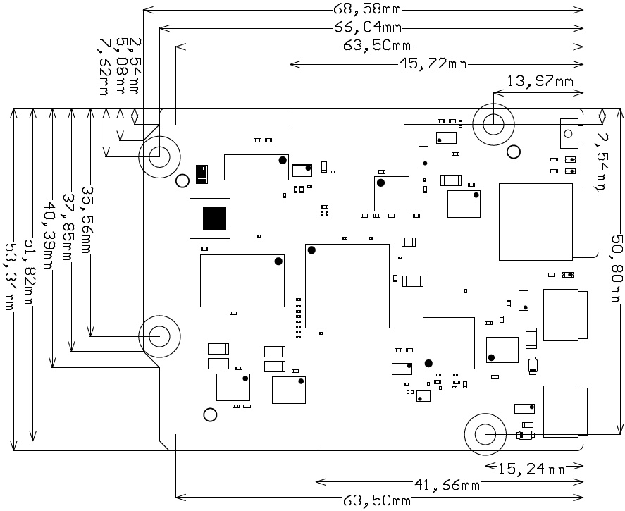
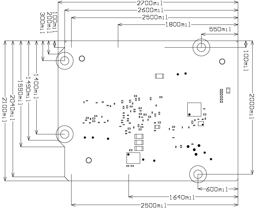
Module size: 68.58 mm × 53.34 mm. Please download the assembly diagram for exact numbers.
PCB thickness: 1.6 mm.
Highest part on PCB: approx. 4 mm. Please download the step model for exact numbers.
Please note that two different units are used on the figures below, SI system millimeters (mm) and imperial system thousandths of an inch(mil). To convert mils to millimeters and vice versa use formula 100mil's = 2,54mm.
Commercial grade: 0°C to +70°C.
Industrial grade: -40°C to +85°C.
Operating temperature range depends also on customer design and cooling solution. Please contact us for options.
... g - Plain module
... g - Set of bolts and nuts
| Date | Revision | Notes | PCN | Documentation Link |
|---|---|---|---|---|
| 2016-07-15 | 03 | Click to see PCN. | TE0723-03 | |
2015-11-06 | 02 | TE0723-02 | ||
01 |
|
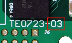
Hardware revision number is printed on the PCB board together with the module model number separated by the dash.
Date | Revision | Contributors | Description |
|---|---|---|---|
| 2017-02-11 | Jan Kumann | Initial document. |