Table of Contents
Download PDF version of this document. |
Table of Contents |
Refer to https://shop.trenz-electronic.de/ee/Download/?path=Trenz_Electronic/TE0841 for downloadable version of this manual and additional technical documentation of the product. |
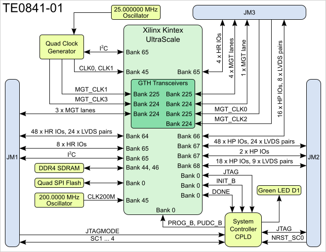
The Trenz Electronic TE0841-01 is an industrial-grade 4 x 5 cm SoM integrating Xilinx Kintex UltraScale KU035 FPGA, 2 banks of 512 MByte DDR4 SDRAM, 32 MByte QSPI Flash for configuration and operation, and powerful switch-mode power supplies for all on-board voltages. Numerous configurable I/Os are provided via rugged high-speed strips. All this on a tiny footprint, smaller than a credit card size at very competitive price. All Trenz Electronic SoMs in 4 x 5 cm form factor are mechanically compatible.
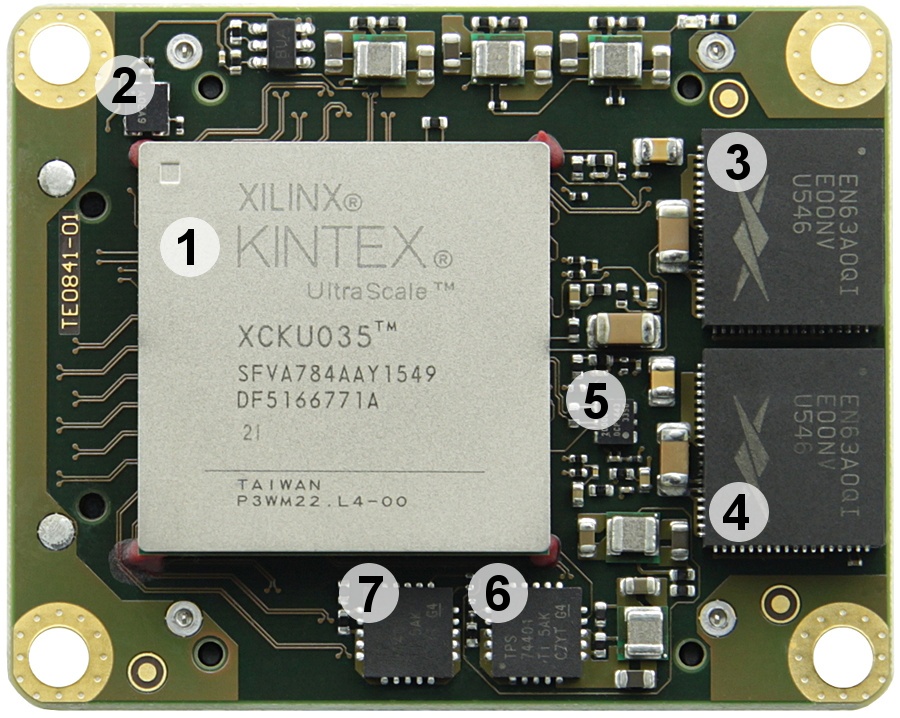
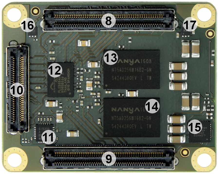
Additional assembly options for cost or performance optimization plus high volume prices are available on request.
Storage device name | Content | Notes |
|---|---|---|
OTP Flash area | ... | |
I/O signals connected from the SoCs I/O banks and B2B connectors:
| FPGA Bank | Type | B2B Connector | I/O Signal Count | Voltage | Notes |
|---|---|---|---|---|---|
| 64 | HR | JM1 | 48 IOs, 24 LVDS pairs | B64_VCCO | Supplied by the baseboard. |
| 65 | HR | JM1 | 8 IOs | 3.3V | |
| 224 | MGT | JM1 | 3 lanes | ||
| 65 | HR | JM3 | 4 IOs, 2 LVDS pairs | 3.3V | |
| 66 | HP | JM3 | 16 IOs, 8 LVDS pairs | B66_VCCO | Supplied by the baseboard |
| 224 | MGT | JM3 | 1 lane | ||
| 225 | MGT | JM3 | 4 lanes | ||
| 67 | HP | JM2 | 48 IOs, 24 LVDS pairs | B67_VCCO | Supplied by the baseboard |
| 67 | HP | JM2 | 2 IOs | B67_VCCO | Supplied by the baseboard |
| 68 | HP | JM2 | 18 IOs, 9 LVDS pairs | B68_VCCO | Supplied by the baseboard |
For detailed information about the pin out, please refer to the Pin-out Tables.
On-board I2C devices are connected to MIO.. and MIO.. which are configured as I2C... by default. I2C addresses for on-board devices are listed in the table below:
| I2C Device | I2C Address | Notes |
|---|---|---|
| Si5338, U2 | 0x70 | Connected to FPGA bank 65. |
JTAG access to the Xilinx Kintex UltraScale FPGA is available through B2B connector JM2.
JTAG Signal | B2B Connector Pin |
|---|---|
| TMS | JM2-93 |
| TDI | JM2-95 |
| TDO | JM2-97 |
| TCK | JM2-99 |
| JTAGMODE pin 89 in B2B connector JM1 should be kept low or grounded for normal operation. |
Special purpose pins are connected to smaller System Controller CPLD and have following default configuration:
| Pin Name | Mode | Function | Default Configuration |
|---|---|---|---|
| JTAGMODE | Input | JTAG select | Low for normal operation. |
| NRST_SC0 | Input | Reset | |
| SC1 | - | - | Not used by default. |
| SC2 | - | - | Not used by default. |
| SC3 | - | - | Not used by default. |
| SC4 | - | - | Not used by default. |
| LED | Color | Connected to | Description and Notes |
|---|---|---|---|
| D1 | Green | System Controlled CPLD, bank 3 | Exact function is defined by SC CPLD firmware. |
| Name | IC | ID | PS7 | MIO | Notes |
|---|---|---|---|---|---|
| Clock | Frequency | IC | FPGA | Notes |
|---|---|---|---|---|
There is a Si5338 programmable quad clock generator chip on-board.
PLL outputs
| I/O | Default Frequency | Notes |
|---|---|---|
| CLK0 | Connected to FPGA pins P23/R23 as CLK1. | |
| CLK1 | Connected to MGT_CLK1. | |
| CLK2 | Connected to MGT_CLK3. | |
| CLK3 | Connected to FPGA pins T24/T25 as CLK0. |
Power supply with minimum current capability of 4A for system startup is recommended.
Power Consumption
| Power Input Pin | Max Current |
|---|---|
| VIN | TBD* |
| 3.3VIN | TBD* |
* TBD - To be determined soon with reference design setup.
For highest efficiency of on board DC-DC regulators, it is recommended ...
Voltages on B2B Connectors | B2B JM1 Pins | B2B JM2 Pins | Input/Output | Notes |
|---|---|---|---|---|
| VIN | 1, 3, 5 | 2, 4, 6, 8 | Input | Supply voltage. |
| 3.3VIN | 13, 15 | - | Input | Supply voltage. |
| B64_VCO | 9, 11 | - | Input | HR (High Range) bank voltage. |
| B66_VCO | - | 1, 3 | Input | HP (High Performance) bank voltage. |
| B67_VCO | - | 7, 9 | Input | HP (High Performance) bank voltage. |
| B68_VCO | - | 5 | Input | HP (High Performance) bank voltage. |
VBAT_IN | 79 | - | Input | RTC battery supply voltage. |
| 3.3V | - | 10, 12, 91 | Output | Module on-board 3.3V voltage level. |
| Module Variant | FPGA Chip | MGT/PL Clock [MHz] |
|---|---|---|
| TE0841-01-035-1C | XCKU035-1SFVA784C | |
TE0841-01-035-1I | XCKU035-1SFVA784I | |
TE0841-01-035-2I | XCKU035-2SFVA784I |
Parameter | Min | Max | Units | Reference Document |
|---|---|---|---|---|
VIN supply voltage | V | - | ||
Storage temperature | -40 | +85 | °C | - |
| Parameter | Min | Max | Units | Reference Document |
|---|---|---|---|---|
| VIN supply voltage |
| Assembly variants for higher storage temperature range are available on request. |
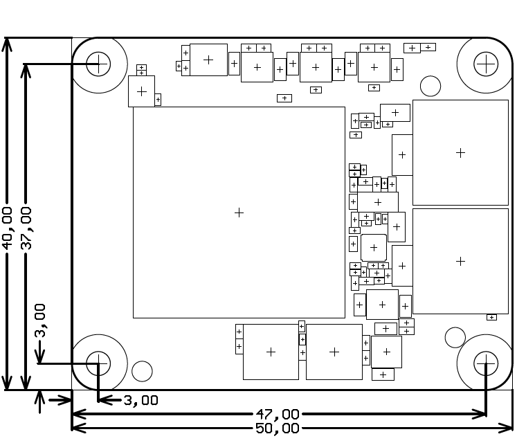
Module size: 50 mm × 40 mm. Please download the assembly diagram for exact numbers.
Mating height with standard connectors: 8 mm.
PCB thickness: 1.6 mm.
Highest part on PCB: approximately 3 mm. Please download the step model for exact numbers.
All dimensions are given in millimeters.
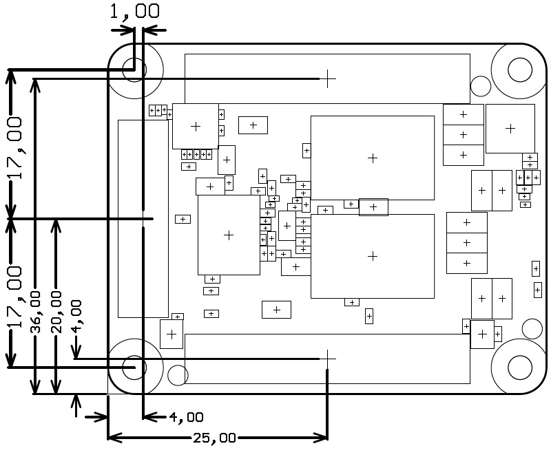
Commercial grade: 0°C to +70°C.
Industrial grade: -40°C to +85°C.
Operating temperature range depends also on customer design and cooling solution. Please contact us for options.
25 g - Plain module.
9 g - Set of bolts and nuts.
| Date | Revision | Notes | PCN | Documentation Link |
|---|---|---|---|---|
| 2015-12-09 | 01 | First production revision | - | TE0841-01 |
Hardware revision number is printed on the PCB board together with the module model number separated by the dash.
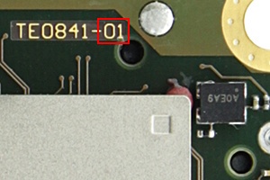
Date | Revision | Contributors | Description |
|---|---|---|---|
| 2017-01-31 | Jan Kumann | Initial document. |