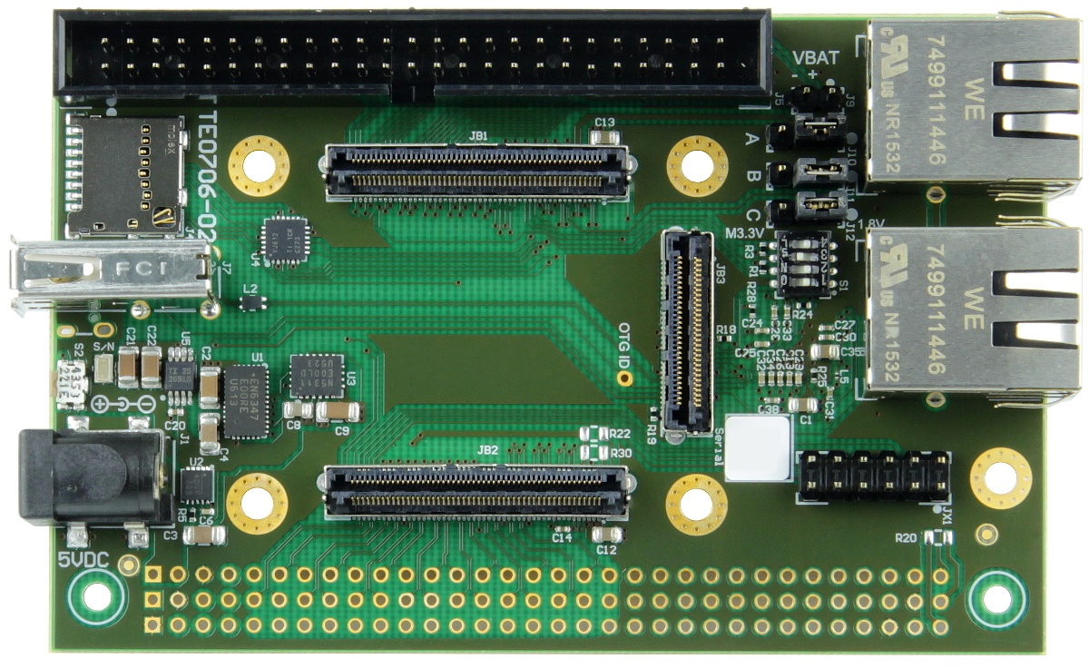

TE0706 is mainly for the use with TE0720 or TE0715 modules. It is possible to use with other 4x5 modules as well, but the usable functionality may be less.
| Function | TE0711 | TE0715 | TE0720 | |||
|---|---|---|---|---|---|---|
| J3: RJ45 | - | PS ETH0 | PS ETH0 | |||
| J2: RJ45 | - | PL ETH | PL ETH | |||
| J4; MicroSD | PS SDIO0 | PS SDIO0 | ||||
| J7: USB | FT2232H* | PS USB0 | PS USB0 | |||
| GTP/GTX | n/a | no | n/a |
When using standard assembly option TE0706 then TE0711 Device side USB will appear in USB Host connector!
TE0715-30 uses Kintex based SoC and has only one 3.3V tolerant bank. Note: TE0706-01 schematic uses net names from TE0720, they are do not have relation to net names and banks if TE0715 is used.
| TE0715-30 | VCCIO max | Connector B2B | VG96 Pin | Notes |
|---|---|---|---|---|
| B13 | 3.3 | JB1.10 JB.12 | B32 | Can solder R20 to use 3.3V in TE0715 bank B13 |
| B34 | 1.8V | JB2.6 | - | Must be connected with fly wire on TE0706, not accessible on the connector |
| B35 | 1.8V | JB2.8 /JB2.10 | B1 | Must connect 1.8V max either wire or from VG96 connector |
With standard delivery of the TE0706, TE0715 would have all 3 FPGA I/O Banks not powered.
| # | Schematic name | Default | |
|---|---|---|---|
| 1 | - | N/A | |
| 2 | PROGMODE | ON | Keep ON for Module JTAG normal operation |
| 3 | MODE | USER | Connected to Module MODE pin, select boot mode, see module documentation |
| 4 | EN1 | OFF |
Size: 65 x 100 mm