• Module: TRM Name always "TE Series Name" +TRM
    Example: "TE0728 TRM"

Template Change history:

DateVersionChangesAuthor

4.2
  • Changes Xilinx to AMD
ED

4.1
  • Minor changes
    • Notes
    • Tables
ED

4.0
  • Rework for smaller TRM which can be generated faster
    • Reduce Signal Interfaces Pin
    • Reduce On Board Periphery
    • Reduce Power
    • Move Configuration Signals from Overview to own section
JH

3.12
  • Version History
    • changed from list to table
  • all
    • changed title-alignment for tables from left to center
ma

3.11
  • update "Recommended Operating Conditions" section


3.1
  • New general notes for temperature range to "Recommended Operating Conditions"


3.02
  • add again fix table of content with workaround to use it for pdf and wiki
  • Export Link for key features examples
    • Notes for different Types (with and without Main FPGA)
  • Export Link for Signals, Interfaces and Pins examples
    • Notes for different Types (Modul, Modul Hybrid, Evalboard, Carrier)


3.01
  • remove fix table of content and page layout ( split page layout make trouble with pdf export)
  • changed and add note to signal and interfaces, to on board periphery section
  • ...(not finished)


3.00
  • → separation of Carrier/Module and evaluation kit TRM


2.15
  • add excerpt macro to key features


2.14
  • add fix table of content
  • add table size as macro


Important General Note:

  • If some section is configurable and depends on Firmware, please refer to the addition page (for example CPLD). If not available, add note, that this part is configurable
  • Designate all graphics and pictures with a number and a description, Use "Scroll Title" macro

    • Use "Scroll Title" macro for pictures and table labels. Figure number must be set manually at the moment (automatically enumeration is planned by scrollPDF)
      • Figure template:


        Create DrawIO object here: Attention if you copy from other page, objects are only linked.


        image link to the generate DrawIO PNG file of this page. This is a workaround until scroll pdf export bug is fixed


      • Table template:

        • Layout macro can be use for landscape of large tables

      • ExampleComment
        12


    • The anchors of the Scroll Title should be named consistent across TRMs. A incomplete list of examples is given below

      • <type>_<main section>_<name>

        • type: Figure, Table
        • main section:
          • "OV" for Overview
          • "SIP" for Signal Interfaces and Pins,
          • "OBP" for On board Peripherals,
          • "PWR" for Power and Power-On Sequence,
          • "B2B" for Board to Board Connector,
          • "TS" for Technical Specification
          • "VCP" for Variants Currently in Production
          •  "RH" for Revision History
        • name: custom, some fix names, see below
      • Fix names:
        • "Figure_OV_BD" for Block Diagram

        • "Figure_OV_MC" for Main Components

        • "Table_OV_IDS" for Initial Delivery State

        • "Table_PWR_PC" for Power Consumption

        • "Figure_PWR_PD" for Power Distribution
        • "Figure_PWR_PS" for Power Sequence
        • "Figure_PWR_PM" for Power Monitoring
        • "Table_PWR_PR" for Power Rails
        • "Table_PWR_BV" for Bank Voltages
        • "Table_TS_AMR" for Absolute_Maximum_Ratings

        • "Table_TS_ROC" for Recommended_Operating_Conditions

        • "Figure_TS_PD" for Physical_Dimensions
        • "Table_VCP_SO" for TE_Shop_Overview
        • "Table_RH_HRH" for Hardware_Revision_History

        • "Figure_RH_HRN" for Hardware_Revision_Number
        • "Table_RH_DCH" for Document_Change_History
    • Use Anchor in the document: add link macro and add "#<anchorname>
    • Refer to Anchor from external : <page url>#<pagename without space characters>-<anchorname>

-----------------------------------------------------------------------

Note for Download Link of the Scroll ignore macro:

Download PDF version of this document.

Overview

The Trenz Electronic TE0726 is an industrial/extended grade module based on AMD Zynq 7 Series. It is Raspberry Pi form-factor compatible.

Refer to http://trenz.org/te0726-info for the latest online version of this manual and other available documentation.

Notes :

Key Features

Note:
 'description: Important components and connector or other Features of the module
→ please sort and indicate assembly options

See examples for different types <Series Name> TRM Template section examples#%3CSeriesName%3ETRMTemplatesectionexamples-KeyFeatures

  • SoC/FPGA/Module
    • Package:                      CLG225
    • Device:                        Z-7007S, Z-7010, 1)
    • Temperature ranges:  Commercial / Extended / Industrial 1)
    • Speed grades:            -3, -2, -1 1)

  • RAM/Storage
    • 512 MByte DDR3L ECC RAM 1)
    • 16 MByte QSPI Flash 1)
    • 2 KBit EEPROM for FTDI
    • 2 KBit EEPROM for Ethernet & USB HUB
  • On Board
    • System Controller CPLD
    • USB ULPI Transceiver
    • 10/100 Ethernet Transceiver with USB hub
    • USB to JTAG / UART FTDI
  • Interface
    • 1x Micro USB (UART/JTAG)
    • 4x USB 2.0
    • 1x microSD Card socket
    • 1x Boot Select DIP switch
    • 1x Ethernet RJ45 socket
    • 1x TRRS Audio Jack 3.5mm with microphone (PWM audio only)
    • 1x HDMI Connector
    • 1x CSI-2 Connector (Camera Serial Interface)
    • 1x DSI Connector (Display Serial Interface)
    • 1x5 Pin Header for I²C
    • 2x20 Pin Header with 26 GPIO, 1x I²C , 5 and 3.3 V
    • 3 additional Pinheaders for CPLD access, Reset and PUDC (SoC Boot IO State) changes
  • Power
    • via Micro USB
    • via 5V Pin header
  • Dimension
    • 56 mm x 85 mm, like Raspberry Pi
  • Notes
    1) Depends on assembly variant

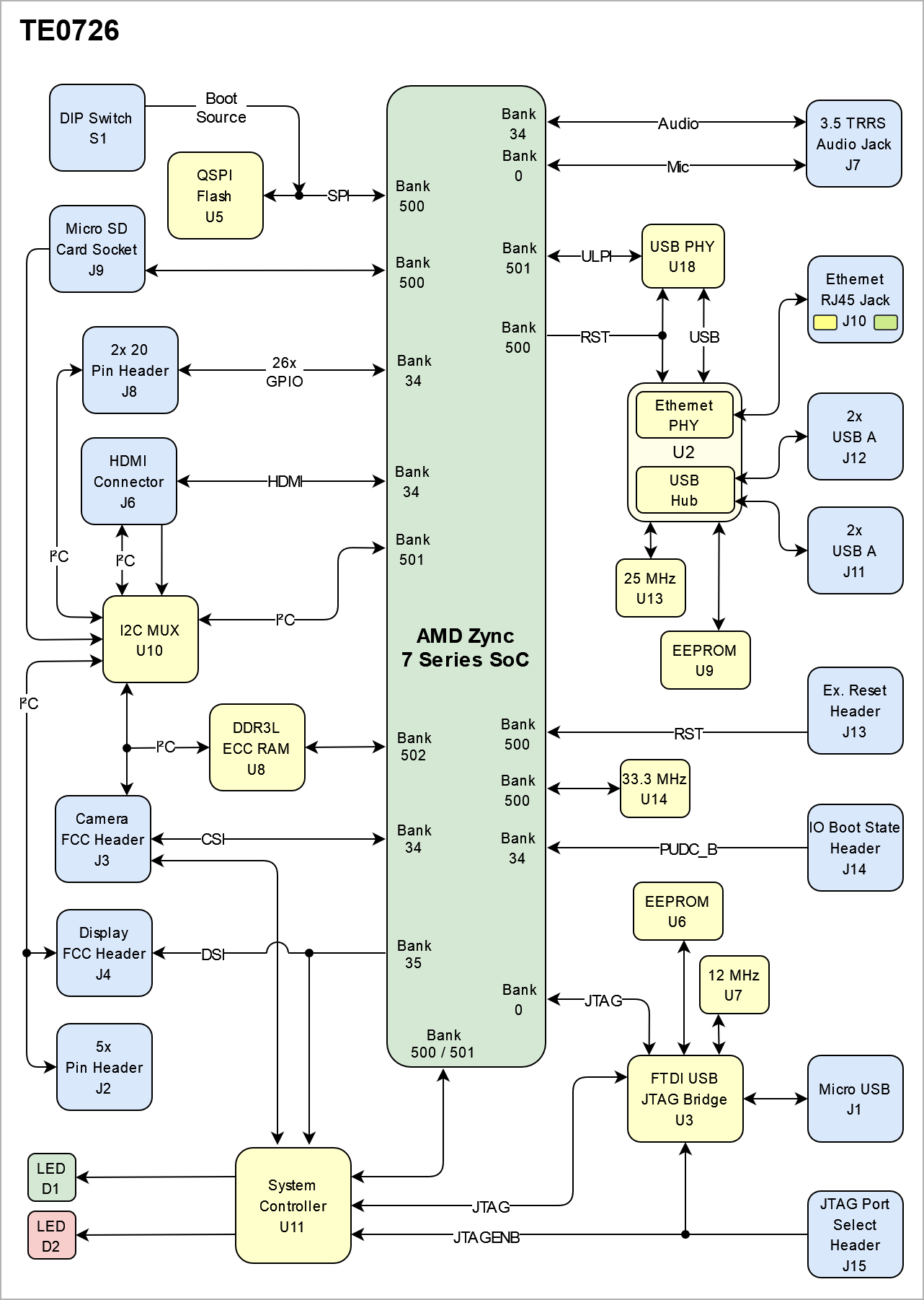
Block Diagram

add drawIO object in Scroll Ignore section and add reference image in Scroll Only.

For more information regarding how to draw a diagram, Please refer to "Diagram Drawing Guidline" .


Title (not anchor) of all Scroll Title such as DrawIOs and Tables should be changed according to the Module name.

Example: TE0812 Block Diagram


All created DrawIOs  should be named according to the Module name:

Example: DrawIO of TE0812 Block Diagram should be named TE0812_OV_BD


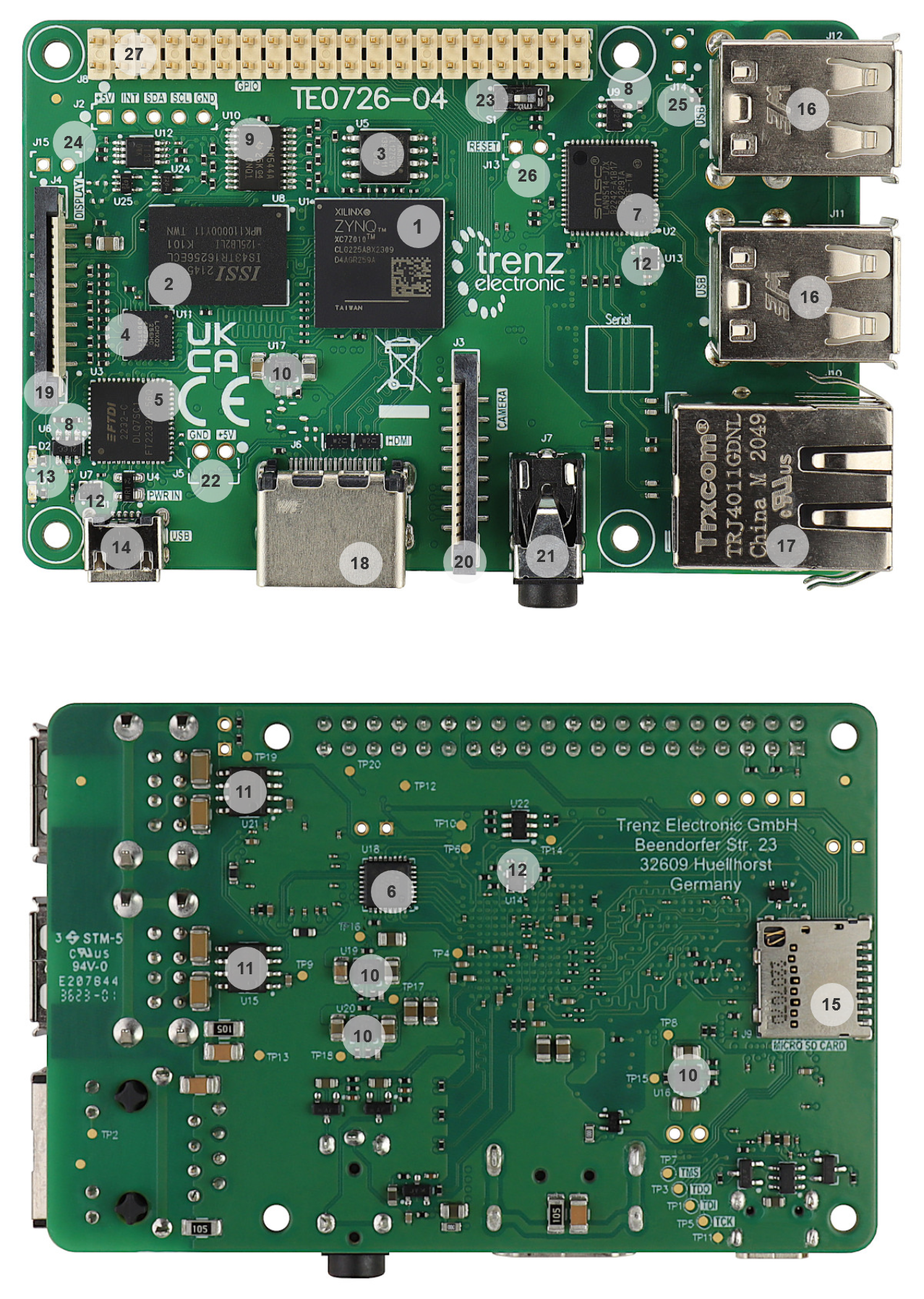
Main Components

For more information regarding how to add board photos, Please refer to "Diagram Drawing Guidline" .


  1. AMD 7 Series Zynq,  U1
  2. DDR3L ECC RAM,  U8
  3. SPI Flash,  U5
  4. System Controller CPLD,  U11
  5. FTDI USB to multipurpose JTAG/FIFO,  U3
  6. USB Transceiver,  U18
  7. Ethernet Transceiver LAN9514 with 4 port USB Hub ,  U2
  8. EEPROM,  U6 , U9
  9. I2C Multiplexer,  U10
  10. Power Supply,  U16, U17, U19, U20
  11. USB power switch,  U15 , U21
  12. Oscillator, U14 , U13 , U7
  13. LED,  D1 , D2
  14. Micro USB B receptacle,  J1
  15. microSD card,  J9
  16. 2x USB A,  J11 , J12
  17. RJ-45 Ethernet connector,  J10
  18. HDMI connector,  J6
  19. DSI LCD connector,  J4
  20. CSI camera connector,  J3
  21. 3.5mm RCA audio jack,  J7
  22. +5V Power Connector,  J5
  23. Boot DIP switch, S1
  24. JTAG Port select header,  J15
  25. Boot IO State select header,  J14
  26. Externer reset header,  J13
  27. 2x20 pin header,  J8

Initial Delivery State


Only components like EEPROM, QSPI flash can be initialized by default at manufacture.

If there is no components which might have initial data ( possible on carrier) you must keep the table empty


Storage device name

Content

Notes

Quad SPI Flash

 not programmed


EEPROM FTDI preprogrammed


EEPROM ETH not programmed
System Controller CPLD preprogrammed


Signals, Interfaces and Pins

For subsection examples see: <Series Name> TRM Template section examples#%3CSeriesName%3ETRMTemplatesectionexamples-Signals,InterfacesandPins

  • Table with all connectors and Designator
  • List of different interfaces per connector
  • IO CNT (for FPGA IOs where functionality can be changed by customer)


Connectors

Connector TypeDesignatorInterfaceIO CNTNotes
2x 20 2.54 mm Pin HeaderJ8

GPIO (HR)

26
2x 20 2.54 mm Pin HeaderJ8I²C2Multiplexer U10

2x 2.54 mm Pin Header

J15

JTAG select

1SoC or SC select

2x 2.54 mm Pin Header

J14

Boot IO State
select

1

2x 2.54 mm Pin Header

J13

External reset

1

2x USB A stacked

J11, J12

USB 2.0

12To USB PHY (ULPI)

5x 2.54 mm Pin Header

J2

I²C

2

Multiplexer U10,
I²C shared with J4

5x 2.54 mm Pin Header

J2

Interrupt

1Multiplexer U10
DIP switchS1

Boot select

1

Shared with SPI

FCC

J4

MIPI DSI

6 (3 pairs)


FCC

J4

I²C

2

Multiplexer U10
FCCJ3

I²C

2

Multiplexer U10
FCC J3

MIPI CSI-2

8 (4 pairs)


HDMIJ6

HDMI

8 (4 pairs)
HDMIJ6

I²C

2Multiplexer U10
HDMIJ6

Interrupt

1Multiplexer U10

Micro-USB 2.0 B

J1

JTAG

2 (1 pair)SoC or SC selectable
microSD CardJ9

Interrupt

1

Multiplexer U10
microSD Card J9

SD

5


RJ-45 Ethernet

J10

10/100 ETH

12To USB PHY (ULPI)

TRRS 3.5 mm

J7

RCA Audio

2

TRRS 3.5 mm

J7

RCA Mic

1


Test Points

Test PointSignalNotes
TP1TDI
TP23.3V
TP3TDO
TP41.8V

TP5

TCK
TP61.0V
TP7TMS
TP81.35V
TP95V
TP10GND
TP11GND
TP12GND
TP13GND
TP14POR BZync SoC reset signal
TP15PG_1.35VPower good signal
TP16PG_1.8VPower good signal
TP17PG_3.3VPower good signal
TP18PG_1.0VPower good signal
TP19PUDCZynq SoC IO State during boot process
TP20SPI0_DQ3/M0Boot source select signal


On-board Peripherals

Notes :

In the on-board peripheral table "chip/Interface" must be linked to the corresponding chapter or subsection by assigning advance link using: #NameOfTheSection


Chip/InterfaceDesignatorConnected ToNotes

DDR3L RAM

U8
  • Zynq SoC DDR Interface PS Bank 502

System Controller CPLD

U11
  • Zynq SoC MIO Bank 35
  • MIDI DSI J4
  • MIDI CSI J3
  • FTDI U7
  • LEDs

USB-PHY

U18
  • Zynq SoC MIO and Zynq SoC USB ULPI

USB Ethernet Hub

J10
  • USB PHY
  • USB A connectors J11 and J12
  • Power switch for USB A connectors U15, U21
  • ETH connector J10
  • EEPROM U9

FTDI

U3
  • JTAG to System Controller and Zynq SoC
  • EEPROM U6

I²C Expander

U10
  • Zynq MIO (Bus master)
  • DDR3L via Voltage Bridge U12 shared with
    MIDI CSI J3
  • MIDI DSI J4 and Pin Header J2
  • HDMI socket J6
  • Pin header J8

I²C Interrupts

U10
  • Zynq MIO (Bus master)
  • microSD Card socket J9 inseration detection
  • HDMI J6 inseration detection
  • Pin header J2

Oscillator

U14
  • Zynq SoC - PS
33.3 MHz

Oscillator

U9
  • USB PHY
25 MHz

Oscillator

U7
  • FTDI
12 MHz


For example subsections see: <Series Name> TRM Template section examples#%3CSeriesName%3ETRMTemplatesectionexamples-On-boardPeripherals

Configuration and System Control Signals

  • Overview  all Controller signals, like Reset, Boote Mode, JTAG Interface(Connector or USB In case of FTDI)...
  • In case it's connected to CPLD always link to CPLD description and add not from the  current implementation here(in case it's available)


Connector

Signal Name

Direction1)Description
S1SPI0_DDQ3 / MOIN

Boot source switch, SPI flash or SD Card

J13EXTRST , POR_B , nRSTINReset Zynq SoC
J14PUDCINState of Zynq SoC IO lines during boot
J15JMODE , BDBUS7INJTAG endpoint selction, System Controller or Zynq SoC

1) Direction:

    • IN: Input from the point of view of this board.
    • OUT: Output from the point of view of this board.

Power and Power-On Sequence

Enter the default value for power supply and startup of the module here.

  • Order of power provided Voltages and Reset/Enable signals

Link to Schematics, for power images or more details


Power Rails

List of all power rails which are accessible by the customer

  • Main Power Rails and Variable Bank Power


Power Rail Name/ Schematic NameConnector + PinDirection1)Notes
USB_B_Vbus

J1

INDefault power supply 5V 

5V

J5.1

IN/OUT2x Pin Header, intended for alternative powering
5V

J2.1
J8.2 , J8.4

OUT5x Pin Header
2x 20 Pin Header

5V_HDMI

J6.18

OUTHDMI, reverse current protection diode D11

V_BUS_A , V_BUS_B , V_BUS_C , V_BUS_D  

J11.A1 , J11.B1 ,
J12.A1 , J12.B1  

OUT2x USB A socket
3.3VJ8.1 , J8.17
J3.15
J4.15
J9.4
OUT2x 20 Pin Header
FCC CSI
FCC DSI
microSD Card socket

1) Direction:

    • IN: Input from the point of view of this board.
    • OUT: Output from the point of view of this board.

Recommended Power up Sequencing

List baseboard design hints for final baseboard development.


SequenceNet nameRecommended Voltage RangePull-up/downDescriptionNotes
1USB_B_Vbus5V (± 5 %)-

Main Power supply via Micro-USB J1.


Main module power supply. 0.5 A minimum. Power consumption depends mainly on design and cooling solution. If more current is needed use J5 for external power supply.

23.3V--Module generated output voltage.


3---

External components which are connected to J8 should be powered up with 3.3V from module.

See link:
https://docs.amd.com/v/u/en-US/ds187-XC7Z010-XC7Z020-Data-Sheet
, page 8 "PL Power‐On/Off Power Supply Sequencing" for PL IO usage


Technical Specifications

List of all power rails which are accessible by the customer

  • Main Power Rails and Variable Bank Power add boarder one time maximum Rating (Board will damaged)

Absolute Maximum Ratings *)

Power Rail / Schematic NameDescriptionMinMaxUnit
USB_B_VbusDetermined through "USB 2.0 VBUS Max Limits"4.755.5V
5VDetermined through "USB 2.0 VBUS Max Limits"4.755.5V


*) Stresses beyond those listed under Absolute Maximum Ratings may cause permanent damage to the device. These are stress ratings only, which do not imply functional operation of the device at these
   or any other conditions beyond those indicated under Recommended Operating Condition. Exposure to absolute-maximum rated conditions for extended periods may affect device reliability.

Recommended Operating Conditions

This TRM is generic for all variants. Temperature range can be differ depending on the assembly version.  Voltage range is mostly the same during variants (exceptions are possible, depending on custom request)

Operating temperature range depends also on customer design and cooling solution. Please contact us for options.

  • Variants of modules are described here: Article Number Information
  • Modules with commercial temperature grade are equipped with components that cover at least the range of 0°C to 75°C
  • Modules with extended temperature grade are equipped with components that cover at least the range of 0°C to 85°C
  • Modules with industrial temperature grade are equipped with components that cover at least the range of -40°C to 85°C
  • The actual operating temperature range will depend on the FPGA / SoC design / usage and cooling and other variables.

ParameterMinMaxUnitsReference Document
USB_B_Vbus4.755.25VSchematic of this board. SCH-TE0726-04-41C94-A.PDF page 3, table "Supported Voltage Ranges"
5V4.755.25VSchematic of this board. SCH-TE0726-04-41C94-A.PDF page 3, table "Supported Voltage Ranges"


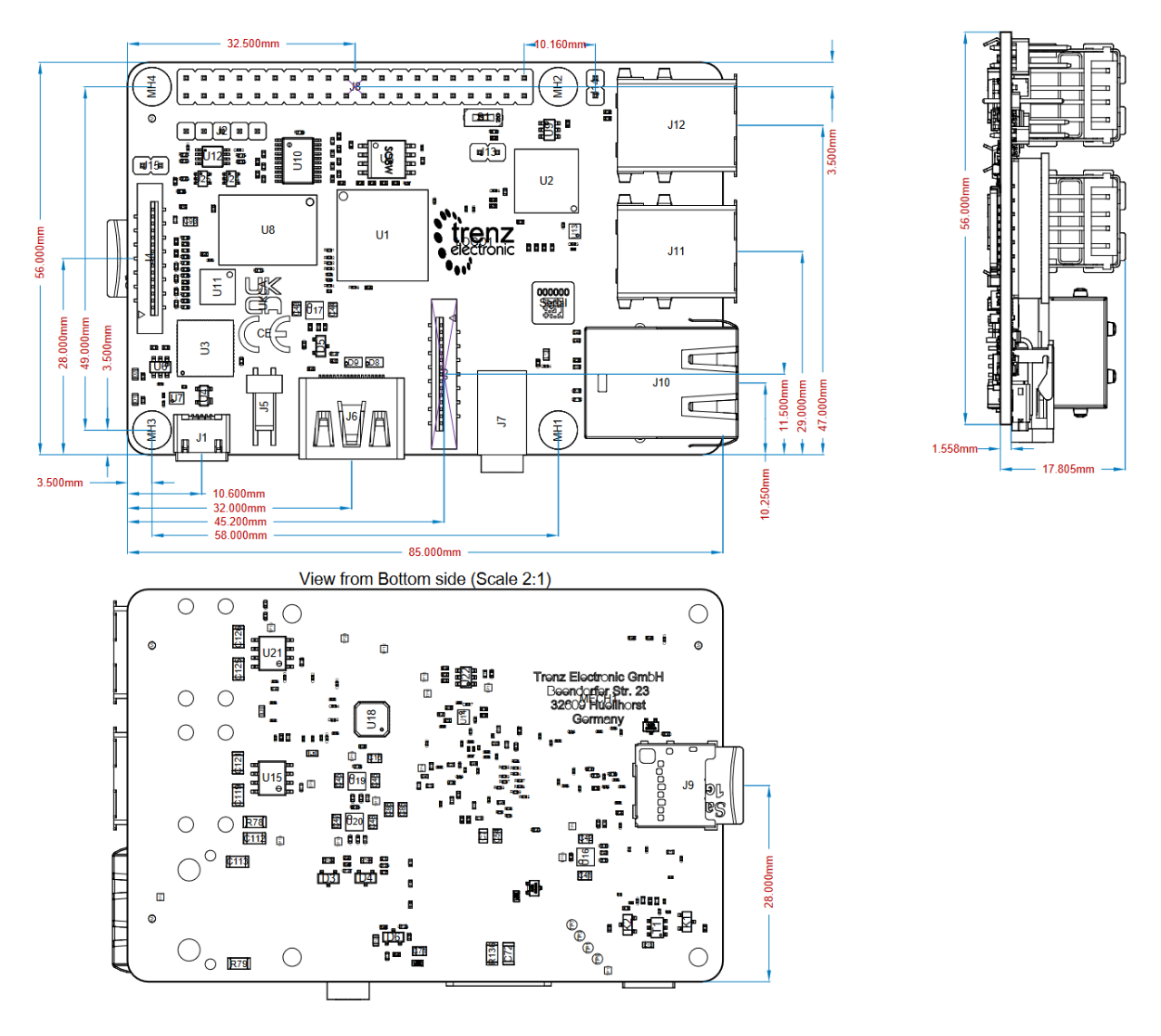
Physical Dimensions

  • Module size: 85 mm × 56 mm.  Please download the assembly diagram for exact numbers.

PCB thickness: 1.57 mm ± 10 %.

In 'Physical Dimension' section, top and bottom view of module must be inserted, information regarding physical dimensions can be obtained through webpage for product in Shop.Trenz, (Download> Documents> Assembly part) for every SoM.

For Example: for Module TE0728, Physical Dimension information can be captured by snipping tools from the link below:

https://www.trenz-electronic.de/fileadmin/docs/Trenz_Electronic/Modules_and_Module_Carriers/5.2x7.6/TE0745/REV02/Documents/AD-TE0745-02-30-1I.PDF

For more information regarding how to draw diagram, Please refer to "Diagram Drawing Guideline" .


Currently Offered Variants 

Set correct link to the shop page overview table of the product on English and German.

Example for TE0706:

    ENG Page: https://shop.trenz-electronic.de/en/search?sSearch=TE0706

    DEU Page: https://shop.trenz-electronic.de/de/search?sSearch=TE0706


Trenz shop TE0726 overview page
English pageGerman page


Revision History

Hardware Revision History

Set correct links to download  Carrier, e.g. TE0706 REV02:

  TE0706-02  ->   https://shop.trenz-electronic.de/Download/?path=Trenz_Electronic/Modules_and_Module_Carriers/4x5/4x5_Carriers/TE0706/REV02/Documents

Note:

  • Date format:  YYYY-MM-DD
  • Example: 

    DateRevisionChangesDocumentation Link
    2020-11-25REV02
    • Resistors R14 and R15 was replaced by 953R (was 5K1)
    • Resistor R5 was replaced by 5K1, R8 by 953R (was 9K09 and 1K69 respectively)
    REV02


DateRevisionChangesPCN LinkDocumentation Link
2023-06-1004

Page Numbers refer to the schematic for this revision

  • EOL components U16, U17 , U19, U20 (EN5311QI) were replaced by MPM3834CGPA
  • Added MIC bias power L12, C114 , R151 (Page 16)
  • Added Legal notices (Page 1)
  • Added power diagram (Page 4)
  • Added S1 switch and R152 for "JTAG only mode" enable (Page 8)
  • The signals were renamed:
    • SPI-DQ0/M0 ---> SPI-DQ0/M3
    • SPI-DQ3/M3 ---> SPI-DQ3/M0
  • ECC function has been added for U8 (Page 11)
  • Added I2C level shifter U12 for DDR3 ECC function (Page 11)
  • Added Buffers U24, U25 to match the level of signals (Page 6)
  • Added Diode D7, resistors R155, R160
  • EOL components L1, L2, L3, L4, L6, L7, L9, L10 BKP0603HS121-T replaced by MPZ0603S121HT000

  • EOL components D8, D9 SP5001-04TTG replaced by EMI8042MUTAG

  • Resistors R80-R82 replaced by 10 kOhm (was 1k43)

  • Added Testpoints TP15 - TP20

  • The type of testpoints TP1 - TP14 was updated. Diameter changed from 0.8 mm to 1 mm

  • CEC function is not supported. L11 was removed. C127, D5, R140, R42 are DNP

  • Power-up sequencing was updated for new DC-DC supplies

  • Capacitors C29, C32, C33 replaced by 470 nF (was 100 nF)

PCN-20230619 TE0726-03 to TE0726-04 Hardware Revision ChangeTE0726-04
2021-01-2103
  • Change DDR3 RAM (U8) from IM4G16D3FABG-125I to IS43TR16256BL-125KBLI
  • Clock Revision Change (U7, U14) from SiT8008AI-... to SiT8008BI-...
  • Clock Revision Change (U13) from SiT8008AI-... to SiT8008BI-...
  • LEDs D1 and D2 changed to 19-213/G6C-BM1N2/DT and 19-213/R6C-AL1M2VY/3T 
  • Set S/N to not fitted
PCN-20210121 TE0726-03 DDR3 Change and Product UpdateTE0726-03
2019-04-0803
  • VBUS Resistor R94 replaced by 10 kOhm (was 12k1)
-TE0726-03
2016-05-0603
  • Introduced new variants:
    • Default with DDR3L 128 Mb
    • TE0726-03M with DDR3L 512 Mb
    • TE0726-03L with DDR3L 128 Mb, 
      without usb's, eth_phy, RJ-45, CSI, DSI, HDMI and 3.5mm jack connectors
  • Changed FTDI to 56 pins package
  • Moved LED's into Raspberry Pi 3 layout
  • Replaced POWER connector on right angle connector
  • Corected conection PUDC pin
  • Replace HDMI, DSI/CSI connector, USB stacked connectors, RJ-45, power connector)
-TE0726-03
2016-01-2602
  • CSI CLK line moved to MRCC pin, CSI lanes swap
  • CSI camera GPIO moved to MIO GPIO
  • RPi GPIO 14,15 moved from MIO to PL
  • Added 47 µF capacitor for SD Card VCC (required by SD spec) 
  • Added 47 µF capacitor for RPi camera - prevent voltage drop at camera init
  • Fixed MODE pin strapping
  • LED change 0603
  • Added POWER connector 2 pin
  • Change HDMI ESD to ESD+EMI 
  • Fixed HDMI HPD and backpower
  • DSI find solution for LS mode
  • Fixed XADC power caps
  • Changed LPDRR2 to DDR3L
-TE0726-02
 -

01

  • Inital board release
--


Hardware revision number can be found on the PCB board together with the module model number separated by the dash.

Document Change History

  • Note this list must be only updated, if the document is online on public doc!
  • It's semi automatically, so do following
    • Add new row below first

    • Copy "Page Information Macro (date)" Macro-Preview, Metadata Version number, Author Name and description to the empty row. Important Revision number must be the same as the Wiki document revision number Update Metadata = "Page Information Macro (current-version)" Preview+1 and add Author and change description. --> this point is will be deleted on newer pdf export template

    • Metadata is only used of compatibility of older exports


DateRevisionContributorDescription

  • Updated to new TRM style.
  • Updated to board REV04.
2017-11-10
v.52
John Hartfiel
  • rework J8 header
2017-11-10v.51Ali Naseri
  • Updated Power section
  • added Power-Distribution diagram
2017-05-30

v.40

Jan Kumann
  • Absolute maximum ratings
  • Layout redesign
  • Wiki link fixed
  • SoC model removed from BD

2017-05-24

v.1

Jan Kumann

  • Initial version

--

all

  • --


Disclaimer


<style>
.wiki-content .columnLayout .cell.aside {
width: 0%;
}</style>


Table of contents