Table of Contents
Download PDF version of this document. |
Table of Contents |
Refer to https://shop.trenz-electronic.de/de/Download/?path=Trenz_Electronic/TE0820 for downloadable version of this manual and additional technical documentation of the product. |
All this on a tiny footprint, smaller than a credit card, at the most competitive price.
All Trenz Electronic SoMs in 4 x 5 cm form factor are mechanically compatible.


3A PFET load switch with configurable slew rate, fast transient isolation and hysteresis control, Q1
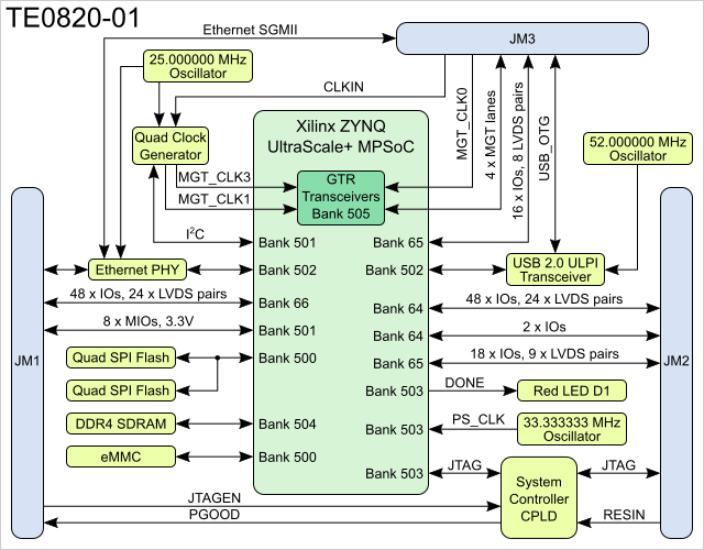
I/O signals connected to the MPSoC's I/O bank and B2B connector:
| Bank | Type | B2B Connector | I/O Signal Count | Voltage | Notes |
|---|---|---|---|---|---|
64 | HP | JM2 | 48 | User | Max voltage 1.8V. |
64 | HP | JM2 | 2 | User | Max voltage 1.8V. |
| 65 | HP | JM2 | 18 | User | Max voltage 1.8V. |
65 | HP | JM3 | 12 | User | Max voltage 1.8V. |
66 | HP | JM1 | 48 | User | Max voltage 1.8V. |
501 | MIO | JM1 | 6 | 1.8V | - |
505 | GTR | JM3 | 4 lanes | N/A | - |
505 | GTR CLK | JM3 | 2 differential inputs | N/A | - |
For detailed information about the pin out, please refer to the Pin-out Table.
System Controller I/O Pins
On-board LEDs
Default MIO Mapping
Gigabit Ethernet
USB Interface
I2C Interface
Boot Modes
Processing System (PS) Peripherals
Clocking
Power Supply
Power-on sequence
Power Rails
Bank Voltages
Parameter | Min | Max | Units | Notes | Reference document |
|---|---|---|---|---|---|
VIN supply voltage | -0.1 | 3.6 | V | ||
| I/O Bank supply voltage | -0.5 | 3.6 | V | Xilinx document DS181 | |
| I/O input voltage for FPGA I/O banks | -0.4 | VCCO_X+0.55 | V | Xilinx document DS181 | |
| GT Transceiver | -0.5 | 1.26 | V | Xilinx document DS181 | |
Voltage on module JTAG pins | -0.4 | VCCO_0+0.55 | V | VCCO_0 is 1.8V or 3.3V nominal | Xilinx document DS181 |
Storage temperature | -40 | +85 | °C |
| Parameter | Min | Max | Units | Notes | Reference document |
|---|---|---|---|---|---|
| VIN supply voltage | 3.135 | 3.45 | V | ||
| IO Bank supply voltage for I/O banks | 1.14 | 3.465 | V | Xilinx document DS181 | |
| I/O input voltage for I/O banks | -0.20 | VCCO + 0.20 | V | Xilinx document DS181 | |
| Voltage on module JTAG pins | 3.135 | 3.465 | V | For a module variant with 3.3V CONFIG Bank option | Xilinx document DS181 |
| Please check Xilinx datasheet DS181 for complete list of absolute maximum and recommended operating ratings for the Artix-7. |
Module size: 50 mm × 40 mm. Please download the assembly diagram for exact numbers.
Mating height with standard connectors: 8 mm
PCB thickness: 1.6 mm
Highest part on PCB: approximately 5 mm. Please download the step model for exact numbers.
All dimensions are shown in mm. Additional sketches, drawings and schematics can be found here.
|
|
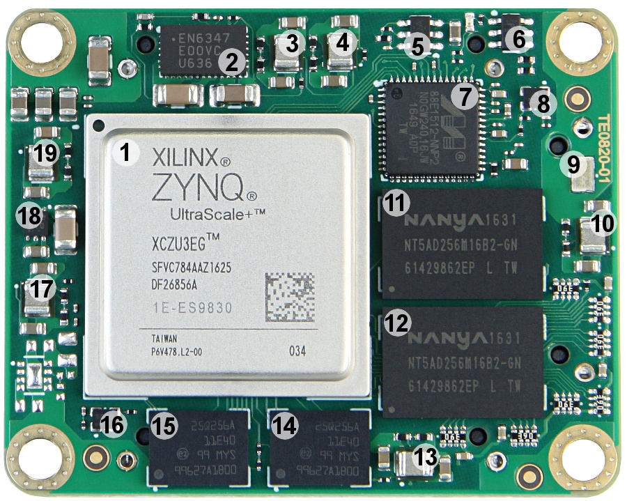
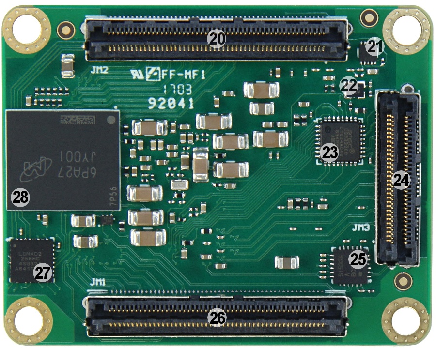
| Top View, Mounting Holes | Bottom View, Samtec Connectors |
Commercial grade modules
All parts are at least commercial temperature range of 0 °C to +70 °C. The module operating temperature range depends on customer design and cooling solution. Please contact us for options.
Industrial grade modules
All parts are at least industrial temperature range of -40 °C to +85 °C. The module operating temperature range depends on customer design and cooling solution. Please contact us for options.
| Variant | Weight in g | Note |
|---|---|---|
| 2IC6 | 8.3 | Plain Module |
| Date | Revision | Notes | PCN Link | Documentation Link |
|---|---|---|---|---|
| 2016-12-23 | 01 | - | TE0820-01 |
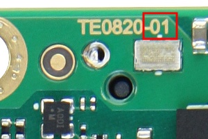
Hardware revision number is printed on the PCB board next to the module model number separated by the dash.

Date | Revision | Authors | Description |
|---|---|---|---|
| 2017-05-10 | Jan Kumann | Initial version. |