Table of Contents
Download PDF version of this document. |
Table of Contents |
Refer to https://shop.trenz-electronic.de/ee/Download/?path=Trenz_Electronic/TE0841 for downloadable version of this manual and additional technical documentation of the product. |
The Trenz Electronic TE0841-01 is an industrial-grade 4 x 5 cm SoM integrating Xilinx Kintex UltraScale KU035 FPGA, 2 banks of 512 MByte DDR4 SDRAM, 32 MByte QSPI Flash for configuration and operation, and powerful switch-mode power supplies for all on-board voltages. Numerous configurable I/Os are provided via rugged high-speed strips. All this on a tiny footprint, smaller than a credit card size at very competitive price. All Trenz Electronic 4 x 5 cm SoMs are mechanically compatible.
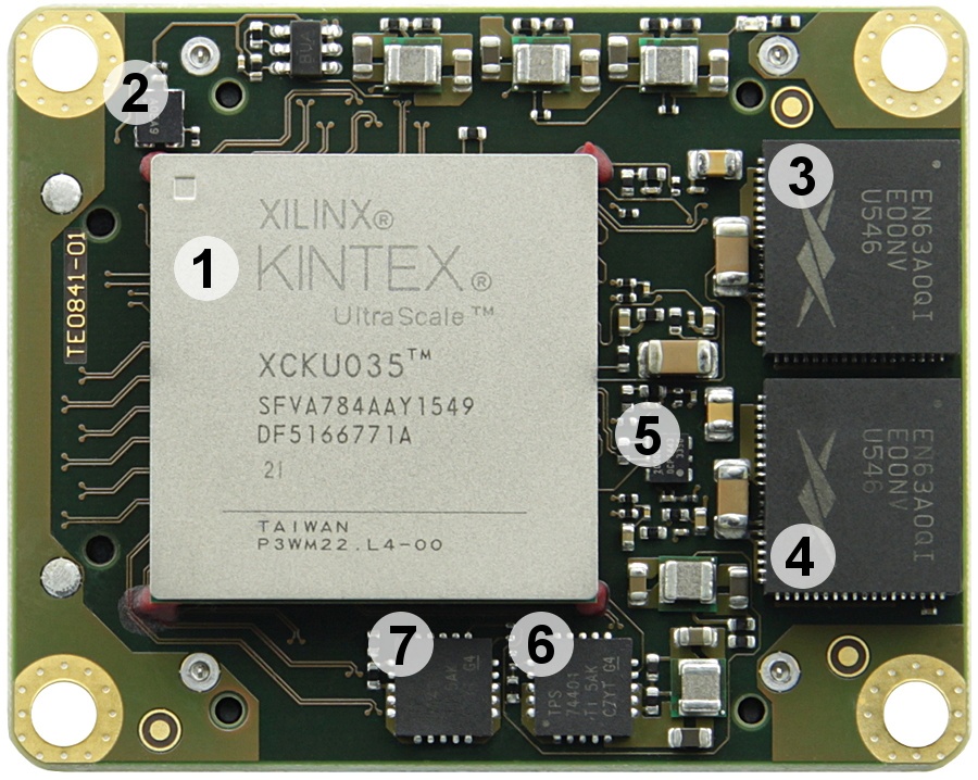
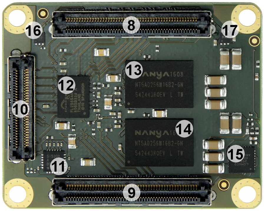
Additional assembly options for cost or performance optimization plus high volume prices are available on request.
Storage device name | Content | Notes |
|---|---|---|
OTP Flash area | Empty |
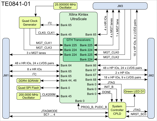
I/O signals connected from the SoCs I/O banks and B2B connectors:
| FPGA Bank | Type | B2B Connector | I/O Signal Count | Voltage | Notes |
|---|---|---|---|---|---|
| 64 | HR | JM1 | 48 IOs, 24 LVDS pairs | B64_VCCO | Supplied by the baseboard. |
| 65 | HR | JM1 | 8 IOs | 3.3V | |
| 224 | MGT | JM1 | 3 lanes | ||
| 65 | HR | JM3 | 4 IOs, 2 LVDS pairs | 3.3V | |
| 66 | HP | JM3 | 16 IOs, 8 LVDS pairs | B66_VCCO | Supplied by the baseboard |
| 224 | MGT | JM3 | 1 lane | ||
| 225 | MGT | JM3 | 4 lanes | ||
| 67 | HP | JM2 | 48 IOs, 24 LVDS pairs | B67_VCCO | Supplied by the baseboard |
| 67 | HP | JM2 | 2 IOs | B67_VCCO | Supplied by the baseboard |
| 68 | HP | JM2 | 18 IOs, 9 LVDS pairs | B68_VCCO | Supplied by the baseboard |
For detailed information about the pin out, please refer to the Pin-out Tables.
There are two PL bank 65 IO pins (PLL_SCL and PLL_SDA) reserved as I2C bus connected to the Si5338 PLL quad clock generator. Default Si5338 PLL chip I2C bus slave address is 0x70.
Additionally, two PL bank 65 IO pins (B65_SCL and B65_SDA) connected to the B2B connector JM1 can be used for external I2C connectivity, otherwise these pins are ordinary IOs.
JTAG access to the Xilinx Kintex UltraScale FPGA is available through B2B connector JM2.
JTAG Signal | B2B Connector Pin |
|---|---|
| TMS | JM2-93 |
| TDI | JM2-95 |
| TDO | JM2-97 |
| TCK | JM2-99 |
| JTAGMODE pin 89 in B2B connector JM1 should be kept low or grounded for normal operation. |
Special purpose pins are connected to the System Controller CPLD and have following default configuration:
| Pin Name | Mode | Function | Default Configuration |
|---|---|---|---|
| JTAGMODE | Input | JTAG select | Low for normal operation. |
| NRST_SC0 | Input | Reset | |
| SC1 | - | - | Not used by default. |
| SC2 | - | - | Not used by default. |
| SC3 | - | - | Not used by default. |
| SC4 | - | - | Not used by default. |
| LED | Color | Connected to | Description and Notes |
|---|---|---|---|
| D1 | Green | System Controller CPLD, bank 3 | Exact function is defined by SC CPLD firmware. |
| Name | IC | ID | PS7 | MIO | Notes |
|---|---|---|---|---|---|
| QSPI Flash | N25Q256A | U6 | |||
| PLL quad clock generator | SI5338A | U2 |
| Clock Signal | Frequency | Source | FPGA | Notes |
|---|---|---|---|---|
| - | 25.000000 MHz | SiT8208 (U3), CLK | - | Reference clock input for Si5338 PLL quad clock generator. |
| CLK200M | 200.0000 MHz | DSC1123 (U11), OUT | R25/R26, bank 45 | |
| CLK0 | User programmable | Si5338 (U2), CLK3 | T24/T25, bank 45 | |
| CLK1 | User programmable | Si5338 (U2), CLK0 | R23/P23, bank 45 | |
| MGT_CLK0 | Baseboard supplied | JM3-31, JM3-33 | Y5/Y6, bank 225 | Bank 225 MGTs clock source from baseboard. |
| MGT_CLK1 | User programmable | Si5338 (U2), CLK1 | V5/V6, bank 225 | Bank 225 MGTs clock source from on-board PLL quad clock generator. |
| MGT_CLK2 | Baseboard supplied | JM3-32, JM3-34 | AD6/AD5, bank 224 | Bank 224 MGTs clock source from baseboard. |
| MGT_CLK3 | User programmable | Si5338 (U2), CLK2 | AB6/AB5, bank 224 | Bank 224 MGTs clock source from on-board PLL quad clock generator. |
Single 3.3V power supply with minimum current capability of 4A for system startup is recommended.
Power Consumption
| Power Input Pin | Max Current |
|---|---|
| VIN | TBD* |
| 3.3VIN | TBD* |
* TBD - To be determined soon with reference design setup.
For highest efficiency of on board DC-DC regulators, it is recommended ...
Voltages on B2B Connectors | B2B JM1 Pins | B2B JM2 Pins | Input/Output | Notes |
|---|---|---|---|---|
| VIN | 1, 3, 5 | 2, 4, 6, 8 | Input | Supply voltage. |
| 3.3VIN | 13, 15 | - | Input | Supply voltage. |
| B64_VCO | 9, 11 | - | Input | HR (High Range) bank voltage. |
| B66_VCO | - | 1, 3 | Input | HP (High Performance) bank voltage. |
| B67_VCO | - | 7, 9 | Input | HP (High Performance) bank voltage. |
| B68_VCO | - | 5 | Input | HP (High Performance) bank voltage. |
VBAT_IN | 79 | - | Input | RTC battery supply voltage. |
| 3.3V | - | 10, 12, 91 | Output | Module on-board 3.3V voltage level. |
| Module Variant | FPGA Chip | PL Clock |
|---|---|---|
| TE0841-01-035-1C | XCKU035-1SFVA784C | |
TE0841-01-035-1I | XCKU035-1SFVA784I | |
TE0841-01-035-2I | XCKU035-2SFVA784I |
Parameter | Min | Max | Units | Reference Document |
|---|---|---|---|---|
VIN supply voltage | V | - | ||
Storage temperature | -40 | +85 | °C | - |
| Parameter | Min | Max | Units | Reference Document |
|---|---|---|---|---|
| VIN supply voltage |
| Assembly variants for higher storage temperature range are available on request. |
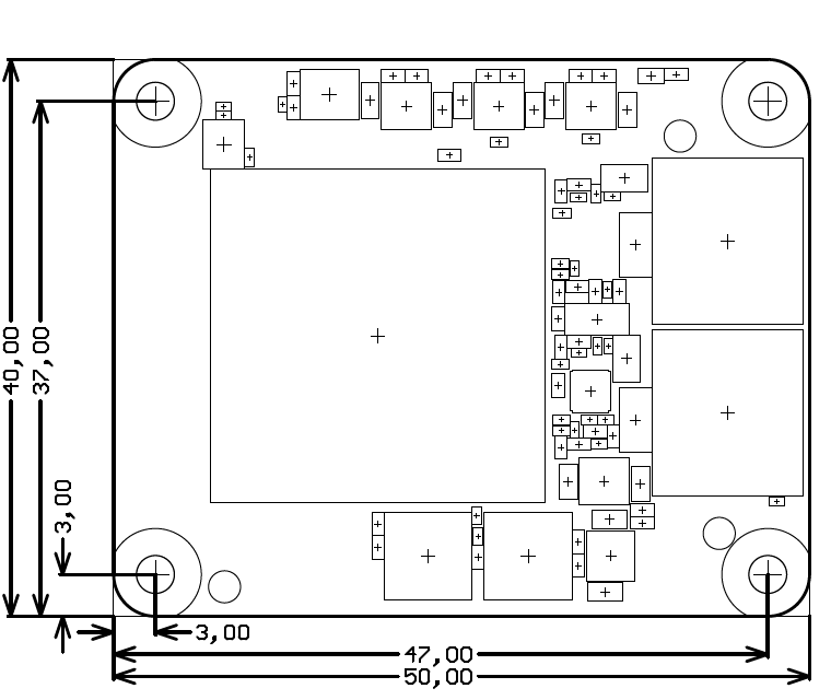
Module size: 50 mm × 40 mm. Please download the assembly diagram for exact numbers.
Mating height with standard connectors: 8 mm.
PCB thickness: 1.6 mm.
Highest part on PCB: approximately 3 mm. Please download the step model for exact numbers.
All dimensions are given in millimeters.
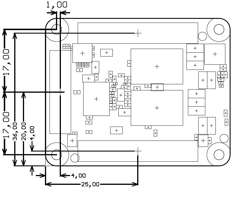
Commercial grade: 0°C to +70°C.
Industrial grade: -40°C to +85°C.
Operating temperature range depends also on customer design and cooling solution. Please contact us for options.
47 g - Plain module.
9 g - Set of bolts and nuts.
| Date | Revision | Notes | PCN | Documentation Link |
|---|---|---|---|---|
| 2015-12-09 | 01 | First production revision | - | TE0841-01 |
Hardware revision number is printed on the PCB board together with the module model number separated by the dash.
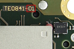
Date | Revision | Contributors | Description |
|---|---|---|---|
| 2017-01-31 | Jan Kumann | Initial document. |