Table of Contents
<!-- Template Revision 1.4 beta (HTML comment will not display, it's not needed to remove them. For Template/Skeleton changes, increase Template Revision number. So we can check faster, if the TRM style is up to date) --> |
Download PDF version of this document. |
Table of Contents |
Refer to https://shop.trenz-electronic.de/en/Download/?path=Trenz_Electronic/carrier_boards/TEBF0808/REV04 for downloadable version of this manual and additional technical documentation of the product. |
The Trenz Electronic TEBF0808 Carrier Board is a baseboard for the Xilinx Zynq Ultrascale+ MPSoC modules TE0808 and TE0803, which exposes the module's B2B connector pins to accessible connectors and provides a whole range of on-board components to test and evaluate the Zynq Ultrascale+ SoMs and for developing purposes.
Additional assembly options are available for cost or performance optimization upon request.

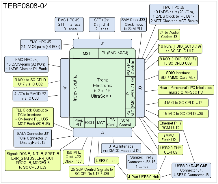
Figure 1: TEBF0808-04 Block Diagram

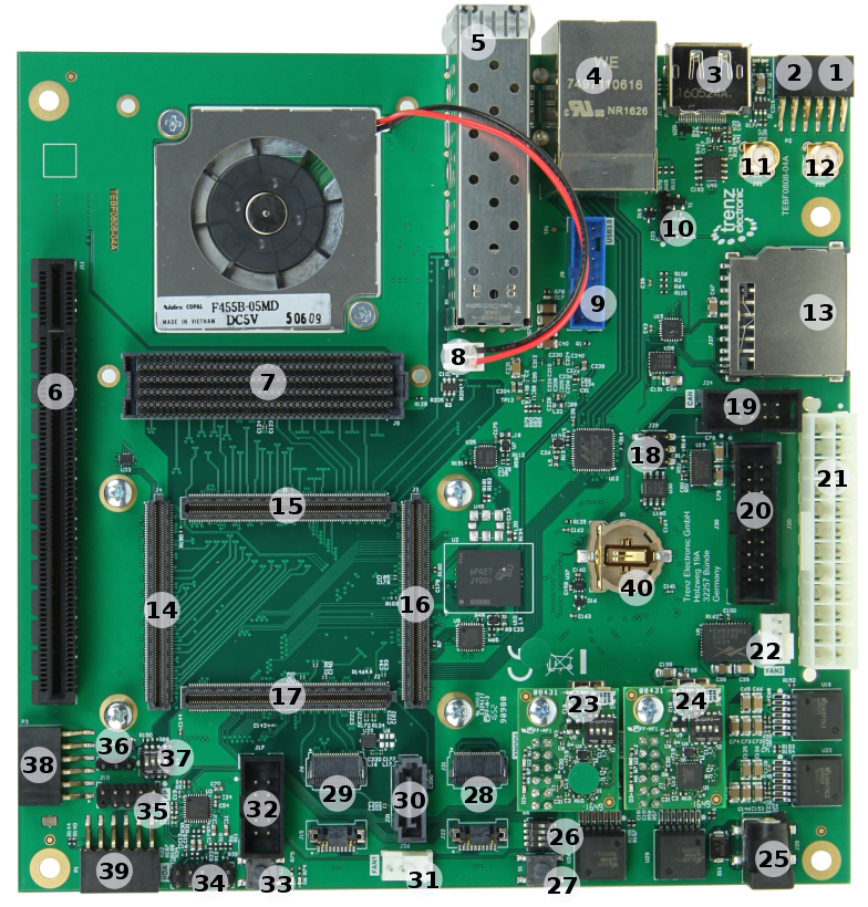
Figure 2: TEBF0808-04 Carrier Board
Storage device name | Content | Notes |
|---|---|---|
General Purpose Configuration EEPROMs (1x Microchip 24LC128-I/ST, 3x Microchip 24AA025E48T-I/OT) | Not programmed | - |
| USB3.0 HUB Configuration EEPROM (Microchip 24LC128-I/ST) | Not programmed | - |
| Si5338A programmable PLL NVM OTP | Not programmed | - |
Table 1: Initial Delivery State of the flash memories
The FMC (FPGA Mezzanine Card) connector J5 with high pin count (HPC) provides as an ANSI/VITA 57.1 standard a modular interface to the MPSoCs FPGA and exposes numerous of its I/O pins for use by other mezzanine modules and expansion cards.
The connector supports single ended (VCCIO: FMC_VADJ) and differential signaling as the I/O's are usable as LVDS-pairs.
The I/O signals are routed from the FPGA banks as LVDS-pairs to the connector:
| FPGA Bank | I/O Signal Count | LVDS-pairs count | VCCO bank Voltage | Reference Clock Input from FMC Connector | Notes |
|---|---|---|---|---|---|
| Bank 48 | 20 | 10 | FMC_VADJ | 1 reference clock signal from FMC connector | - |
| Bank 64 | 46 | 23 | FMC_VADJ | 1 reference clock signal from FMC connector | bank's VREF-pin connected to FMC connector pin J5-H1 (VREF_A_M2C) |
| Bank 65 | 46 | 23 | FMC_VADJ | - | bank's VREF-pin connected to FMC connector pin J5-H1 (VREF_A_M2C) |
| Bank 66 | 48 | 24 | FMC_VADJ | - | bank's VREF-pin connected to FMC connector pin J5-H1 (VREF_A_M2C) |
Table 2: FMC connector pin-outs of available logic banks of the MPSoC
The MGT-banks have also clock input-pins which are exposed to the FMC connector. Following MGT-lanes are available on the FMC connectors J5:
| GT Bank | Type | Count of MGT Lanes | Schematic Names / Connector Pins | MGT Bank's Reference Clock Inputs from FMC Connector |
|---|---|---|---|---|
| 228 | GTH | 4 GTH lanes | B228_RX3_P, B228_RX3_N, pins J5-A10, J5-A11 B228_RX2_P, B228_RX2_N, pins J5-A6, J5-A7 B228_RX1_P, B228_RX1_N, pins J5-A2, J5-A3 B228_RX0_P, B228_RX0_N, pins J5-C6, J5-C7 | 1 reference clock signal (B228_CLK0) from FMC connector |
| 229 | GTH | 4 GTH lanes | B229_RX3_P, B229_RX3_N, pins J5-B12, J5-B13 B229_RX2_P, B229_RX2_N, pins J5-B16, J5-B17 B229_RX1_P, B229_RX1_N, pins J5-A18, J5-A19 B229_RX0_P, B229_RX0_N, pins J5-A14, J5-A15 | 1 reference clock signal (B229_CLK0) from FMC connector |
| 230 | GTH | 2 GTH lanes | B230_RX1_P, B230_RX1_N, pins J5-B4, J5-B5 B230_RX0_P, B230_RX0_N, pins J5-B8, J5-B9 | - |
Table 2: FMC connector pin-outs of available MGT-lanes of the MPSoC
The FMC connector provides pins for reference clock output to the Mezzanine module:
| Clock Signal Schematic Name | FMC Connector Pins | Clock Source | Notes |
|---|---|---|---|
| FMCCLK2 | J5-K4 / J5-K5 | Carrier Board PLL SI5338A U35, CLK2 | - |
| FMCCLK3 | J5-J2 / J5-J3 | Carrier Board PLL SI5338A U35, CLK3 | - |
Table 3: FMC connector pin-outs for reference clock output
The FMC connector provides further interfaces like 'JTAG' and 'I²C' to the System Controller CPLD:
| Interfaces | I/O Signal Count | Pin schematic Names / FMC Pins | Connected to | Notes |
|---|---|---|---|---|
| JTAG | 5 | FMC_TCK, pin J5-D29 FMC_TMS, pin J5-D33 FMC_TDI, pin J5-D30 FMC_TDO, pin J5- D31 | SC CPLD U17, bank 1 | VCCIO: 3V3SB TRST_L, pin J5-D34 pulled-up to 3V3_PER |
| I²C | 2 | FMC_SCL, pin J5-C30 FMC_SDA, pin J5-C31 | I²C-Switch U16 | I²C-lines pulled-up to 3V3_PER |
| Control Lines | 3 | FMC_PRSNT_M2C, pin J5-H2 FMC_PG_C2M, pin J5-D1 (3V3_PER pull-up) FMC_PG_M2C, pin J5-F1 (3V3_PER pull-up) FMC_CLK_DIR, pin J5-B1 (pulled-down to GND) | I²C-Switch U16 via I²C-I/O-Port-Expander U38 SC CPLD U39, bank 0 I²C-Switch U16 via I²C-I/O-Port-Expander U38 SC CPLD U17, bank 1 | 'PG' = 'Power Good'-signal 'C2M' = carrier to (mezzanine) module 'M2C' = (mezzanine) module to carrier |
Table 4: FMC connector pin-outs of available interfaces to the System Controller CPLD
Several VCCIO voltages are available on the FMC connector to operate the I/O's in order of the intended purpose:
| VCCIO Schematic Name | Max. Current | FMC Connector J5 Pins | Notes |
|---|---|---|---|
| 12V | C35/C37 | 12V supply voltage | |
| 3V3_PER | D32/D36/D38/D40/C39 | 3.3V peripheral supply voltage | |
| FMC_VADJ | H40/G39/F40/E39 | adjustable FMC VCCIO voltage, supplied by DCDC converter U8 |
Table 5: Available VCCIO voltages on FMC connector
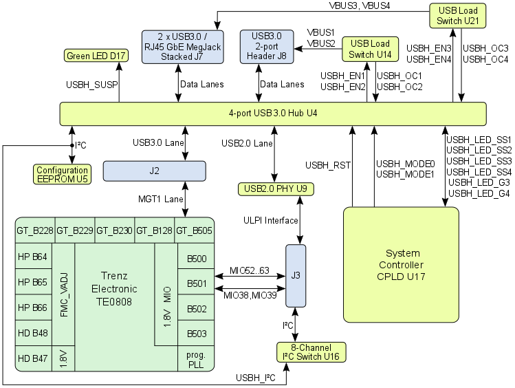
The TEBF0808 Carrier Board offers up to 4 USB3.0 superspeed ports, which are also downward compatible to USB2.0 highspeed ports. The USB3.0 ports are provided by the IC U4, Cypress Semiconductor CYUSB3324 4-port USB3.0 Hub.
On the Upstream-side, this chip is connected to the MGT1-lane of MPSoC's bank 505 to establish the USB3.0 lane. For the USB2.0 interface, the USB3.0 HUB U4 is connected to the on-board USB2.0 PHY U9.
Following block-diagram clarifies the wiring of the USB interface with the MPSoC.

Figure 2: TEBF0808 USB3.0 interface