Table of Contents
<!-- Template Revision 1.68 (HTML comments will be not displayed in the document, no need to remove them. For Template/Skeleton changes, increase Template Revision number. So we can check faster, if the TRM style is up to date). --> |
<!-- General Notes: If some section is CPLD firmware dependent, make a note and if available link to the CPLD firmware description. It's in the TE shop download area in the corresponding module -> revision -> firmware folder. --> |
<!-- General Notes: Designate all graphics and pictures with a number and a description. For example "Figure 1: TE07xx-xx Block Diagram" or "Table 1: Initial delivery state". "Figure x" and "Table x" have to be formatted to bold. --> |
<!-- Link to the base folder of the module (remove de/ or en/ from the URL): for example: https://shop.trenz-electronic.de/Download/?path=Trenz_Electronic/Modules_and_Module_Carriers/4x5/4x5_Carriers/TE0703/ --> |
Download PDF version of this document.
|
Table of Contents |
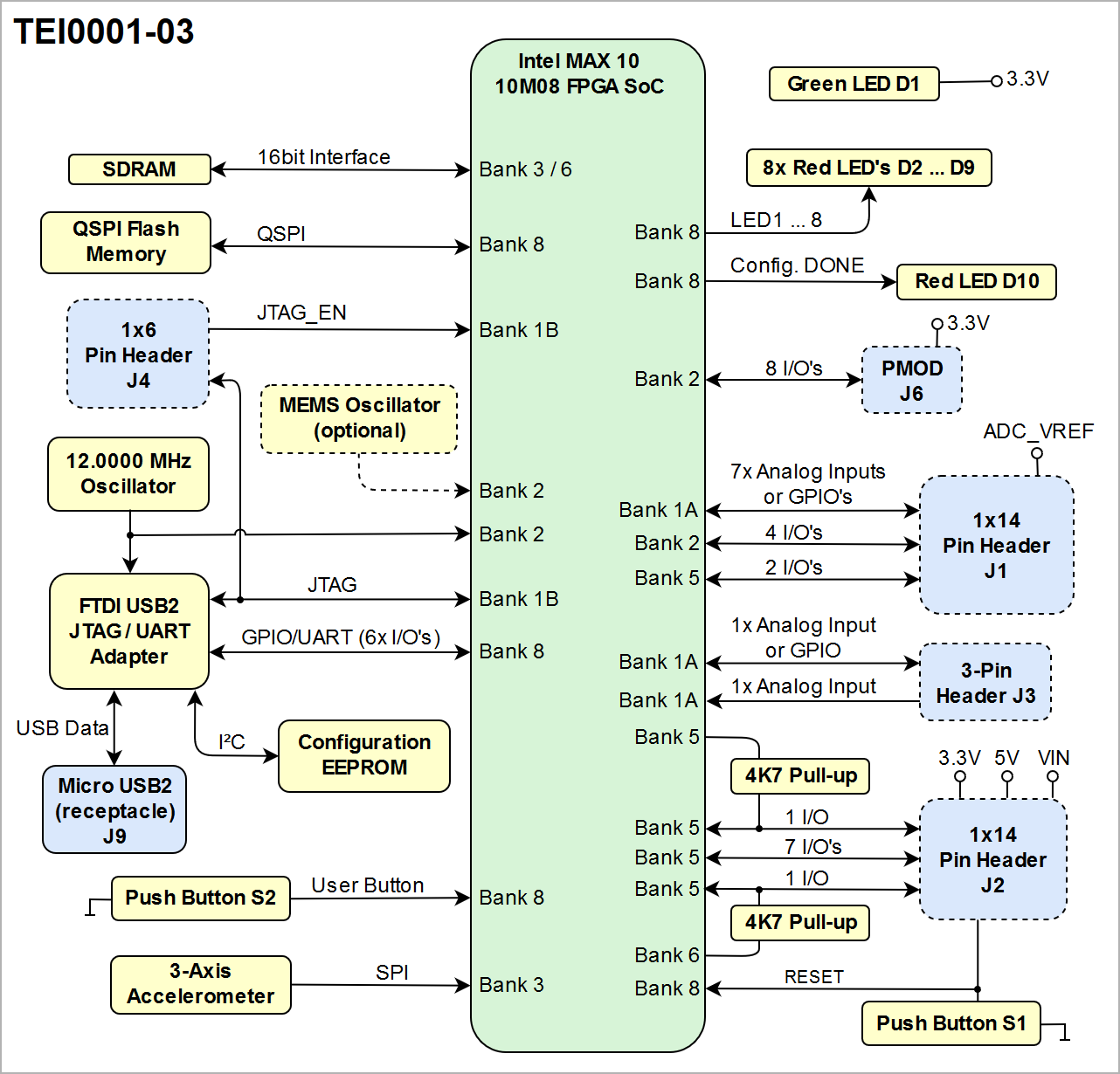
The Trenz Electronic TEI0001 MAX1000 is a low cost small-sized FPGA module integrating a Intel MAX 10 FPGA SoC, 8 MByte serial memory for user application, 8 MByte SDRAM and a 3-axis accelerometer.
<!-- Use short link the Wiki Ressource page: for example: http://trenz.org/te0720-info List of available short links: https://wiki.trenz-electronic.de/display/CON/Redirects --> |
Refer to http://trenz.org/max1000-info for the current online version of this manual and other available documentation. |
Intel MAX 10 10M08 FPGA SoC
8 MByte QSPI Flash memory
2x 14-pin headers (2,54 mm pitch) providing 22 GPIOs with 7 analog inputs as alternative function
8x user LEDs
Additional assembly options are available for cost or performance optimization upon request.
|
|
Storage device name | Content | Notes |
|---|---|---|
Quad SPI Flash, U5 | DEMO Design | - |
| I2C Configuration EEPROM, U9 | Programmed | - |
Table 1: Initial delivery state of programmable devices on the module
The FPGA configuration for Intel MAX 10 FPGAs can be stored through JTAG interface on the FPGA itself since the Intel MAX 10 FPGA offers non-volatile memory on chip. The FPGA configuration is loaded from the non-volatile memory when the board is powered up.
To configure the FPGA directly, the JTAG interface can be used to configure the FPGA volatile, means the configuration is lost after power off.
I/O signals of the FPGA SoC's I/O banks connected to the board's pin headers and connectors:
| Bank | Connector Designator | I/O Signal Count | Bank Voltage | Notes |
|---|---|---|---|---|
| 2 | J1 | 4 I/O's | 3.3V | - |
| J6 | 8 I/O's | Pmod connector | ||
| 5 | J1 | 2 I/O's | 3.3V | - |
| J2 | 9 I/O's | 2 I/O's of bank 5 can be pulled-up to 3.3V (4K7 resistors) | ||
| 1A | J1 | 7x analog inputs or GPIO's, 1x Analog reference voltage (AREF) | 3.3V | analog pins usable as GPIO's as alternative function |
| J3 | 1x analog inputs or GPIO, 1x dedicated analog input | |||
| 1B | J4 | JTAG interface and 'JTAGEN' signal (5 I/O's) | 3.3V | JTAG enable signal (JTAGEN) on pin J4-2, switch between user I/O pins and JTAG pin functions |
Table 2: General overview of single ended I/O signals connected to pin headers and connectors
Table below contains the signals and interfaces of the FPGA banks connected to pins and peripherals of the board:
| Bank | I/O's Count | Connected to | Notes |
|---|---|---|---|
| 2 | 4 | 1x14 pin header, J1 | user GPIO's |
| 8 | Pmod connector, J6 | user GPIO's | |
| 1 | clock oscillator, U7 | 12.0000 MHz reference clock input | |
| 1 | optional clock oscillator, U6 | oscillator not fitted, footprints available for Microchip MEMS oscillator | |
| 5 | 9 | 1x14 pin header, J2 | 2 I/O's (D11, D12) of bank 5 can be pulled-up to 3.3V (4K7 resistors) with 1 I/O (D12_R) of same Bank and 1 I/O (D11_R) of bank 6 |
| 6 | 18 | 8 MByte SDRAM 166MHz, U2 | 16bit SDRAM memory interface |
| 3 | 22 | 8 MByte SDRAM 166MHz, U2 | 16bit SDRAM memory interface |
| 6 | LIS3DH 3-axis accelerometer, U4 | 4 I/O's for SPI interface, 2 interrupt lines | |
| 1A | 8 | 1x14 pin headers J1 | 7 analog inputs or GPIO's, 1 pin analog reference voltage input |
| 2 | pin headers J1 | 1 analog inputs or GPIO, 1 dedicated analog input | |
| 1B | 5 | pin header J4 | 4 I/O's JTAG interface and 1x 'JTAGEN' signal to switch the JTAG pins to user GPIO's if drive this pin to GND |
| 8 | 8 | LEDs D2 ... D9 | Red user LEDs |
| 6 | QSPI Flash memory, U5 | 6 pins Quad SPI interface, 2 of them pulled up as configuration pins during initialization | |
| 6 | FTDI FT2232H JTAG/UART Adapter, U3 | 6 pins configurable as GPIO/UART or other serial interfaces | |
| 1 | Red LED, D10 | Configuration DONE Led (ON when configuration in progress, OFF when configuration is done) | |
| 1 | User button S2 | user configurable | |
| 1 | Reset button S1 and pin J2-10 | low active reset line for FPGA reconfiguration |
Table 3: General overview of FPGA I/O banks
Primary JTAG access to the FPGA SoC device U1 is provided through Micro USB2 B connector J9. The JTAG interface is created by the FTDI FT2232H USB2 to JTAG/UART adapter IC U3.
Optionally 1x6 male pin header J4 can be fitted on board for access to the JTAG interface between FTDI and FPGA on board. The pin assignment of header J4 is shown on table below:
| JTAG Signal | Pin on Header J4 | Note |
|---|---|---|
| TCK | 3 | - |
| TDI | 5 | - |
| TDO | 4 | - |
| TMS | 6 | - |
| JTAGEN | 2 | leave floating when use JTAG interface, otherwise signals on FPGA are GPIOs |
Table 4: optional JTAG pin header
On-board serial configuration memory (U5) is provided by Winbond W74M64FVSSIQ with 64 MBit (8 MByte) storage capacity. This non volatile memory is used to store initial FPGA configuration via JTAG interface. The memory is connected to FPGA bank 1 via SPI interface.
| Serial Memory U5 Pin | Signal Schematic Name | Connected to | Notes |
|---|---|---|---|
| Pin 1, CS | F_CS | FPGA bank 8, pin B3 | chip select |
| Pin 6, CLK | F_CLK | FPGA bank 8, pin A3 | clock |
| Pin 5, SI/IO0 | F_DI | FPGA bank 8, pin A2 | data in / out |
| Pin 7, HOLD/IO3 | NSTATUS | FPGA bank 8, pin C4 | data in / out, configuration dual-purpose pin of FPGA |
| Pin 3, WP/IO2 | DEVCLRN | FPGA bank 8, pin B9 | data in / out, configuration dual-purpose pin of FPGA |
| Pin 2, SO/IO1 | F_DO | FPGA bank 8, pin B2 | data in / out |
Table 5: Quad SPI Flash memory interface
The FPGA module is equipped with a Winbond W9864G6JT 64 MBit (8 MByte) SDRAM chip U2 in standard configuration, variants with 256 Mbit (32 MByte) memory density are also available. The SDRAM chip is connected to the FPGA bank 3 and 6 via 16-bit memory interface with 166MHz clock frequency and CL3 CAS latency.
| SDRAM I/O Signals | Signal Schematic Name | Connected to | Notes |
|---|---|---|---|
| Address inputs | A0 ... A13 | bank 3 | - |
| Bank address inputs | BA0 / BA1 | bank 3 | - |
| Data input/output | DQ0 ... DQ15 | bank 6 | - |
| Data mask | DQM0 ... DQM1 | bank 6 | - |
| Clock | CLK | bank 3 | |
| Control Signals | CS | bank 3 | Chip select |
CKE | bank 3 | Clock enable | |
RAS | bank 3 | Row Address Strobe | |
CAS | bank 3 | Column Address Strobe | |
| WE | bank 3 | Write Enable |
Table 6: 16bit SDRAM memory interface
The FTDI chip U3 converts signals from USB2 to a variety of standard serial and parallel interfaces. Refer to the FTDI data sheet to get information about the capacity of the FT2232H chip.
FTDI FT2232H chip is used in MPPSE mode for JTAG, 6 I/O's of Channel B are routed to FPGA bank 8 of the FPGA SoC and are usable for example as GPIOs, UART or other standard interfaces.
The configuration of FTDI FT2232H chip is pre-programmed on the EEPROM U9.
| FTDI Chip U3 Pin | Signal Schematic Name | Connected to | Notes |
|---|---|---|---|
| Pin 12, ADBUS0 | TCK | FPGA bank 1B, pin G2 | JTAG interface |
| Pin 13, ADBUS1 | TDI | FPGA bank 1B, pin F5 | |
| Pin 14, ADBUS2 | TDO | FPGA bank 1B, pin F6 | |
| Pin 15, ADBUS3 | TMS | FPGA bank 1B, pin G1 | |
| Pin 32, BDBUS0 | BDBUS0 | FPGA bank 8, pin A4 | user configurable |
| Pin 33, BDBUS1 | BDBUS1 | FPGA bank 8, pin B4 | user configurable |
| Pin 34, BDBUS2 | BDBUS2 | FPGA bank 8, pin B5 | user configurable |
| Pin 35, BDBUS3 | BDBUS3 | FPGA bank 8, pin A6 | user configurable |
| Pin 37, BDBUS4 | BDBUS4 | FPGA bank 8, pin B6 | user configurable |
| Pin 38, BDBUS5 | BDBUS5 | FPGA bank 8, pin A7 | user configurable |
Table 7: FTDI chip interfaces and pins
On the TEI0001 FPGA board there is a 3-axis accelerometer present. This accelerometer provided by ST Microelectronics LIS3DH and offers many function to detect motion and has also a temperature sensor integrated. It also has a FIFO buffer for storing output data. The sensor is connected to the FPGA through SPI interface and two interrupt lines.
| Accelerometer U4 Pin | Signal Schematic Name | Connected to | Notes |
|---|---|---|---|
| Pin 11, INT1 | SEN_INT1 | FPGA bank 3, pin J5 | Interrupt lines |
| Pin 9, INT2 | SEN_INT2 | FPGA bank 3, pin L4 | |
| Pin 6, SDA/SDI/SDO | SEN_SDI | FPGA bank 3, pin J7 | SPI interface |
| Pin 7, SDO/SA0 | SEN_SDO | FPGA bank 3, pin K5 | |
| Pin 4, SCL/SPC | SEN_SPC | FPGA bank 3, pin J6 | |
| Pin 8, CS | SEN_CS | FPGA bank 3, pin L5 | |
| Pin 13, ADC3 | ADC3 | 5V | Sense 5V input voltage |
Table 8: 3-axis accelerometer interfaces and pins
The FPGA SoC module has following reference clocking signals provided by on-board oscillators:
| Clock Source | Schematic Name | Frequency | Clock Input Destination |
|---|---|---|---|
| Microchip MEMS Oscillator, U7 | CLK12M | 12.0000 MHz | FTDI FT2232 U3, pin 3; FPGA SoC bank 2, pin H6 |
| optional Microchip MEMS Oscillator, U6 (not fitted) | CLK_X | - | FPGA SoC bank 2, pin G5 |
Table 9: Clock sources overview
There are 10 LEDs fitted on the FPGA module board. The LEDs are user configurable to indicate for example any system status.
| LED | Color | Signal Schematic Name | FPGA | Notes |
|---|---|---|---|---|
| D1 | Green | - | - | Indicating 3.3V board supply voltage |
| D2 | Red | 'LED1' | bank 8, pin A8 | user |
| D3 | Red | 'LED2' | bank 8, pin A9 | user |
| D4 | Red | 'LED3' | bank 8, pin A11 | user |
| D5 | Red | 'LED4' | bank 8, pin A10 | user |
| D6 | Red | 'LED5' | bank 8, pin B10 | user |
| D7 | Red | 'LED6' | bank 8, pin C9 | user |
| D8 | Red | 'LED7' | bank 8, pin C10 | user |
| D9 | Red | 'LED8' | bank 8, pin D8 | user |
| D10 | Red | 'CONF_DONE' | bank 8, pin C5 | indication configuration is DONE when LED is off |
Table 10: LEDs of the module
The FPGA module is equipped with two push buttons S1 and S2:
| Button | Signal Schematic Name | FPGA | Notes |
|---|---|---|---|
| S1 | 'USER_BTN' | bank 8, pin E6 | user configurable |
| S2 | 'RESET' | bank 8, pin E7 | FPGA reset |
Table 11: Push buttons of the module
All connectors are are for 100mil headers, all connector locations are in 100mil (2.54mm) grid. The module's PCB provides footprints to mount and solder optional pin headers, if those are not factory-fitted on module.
To power-up a module, power supply with minimum current capability of 1A is recommended.
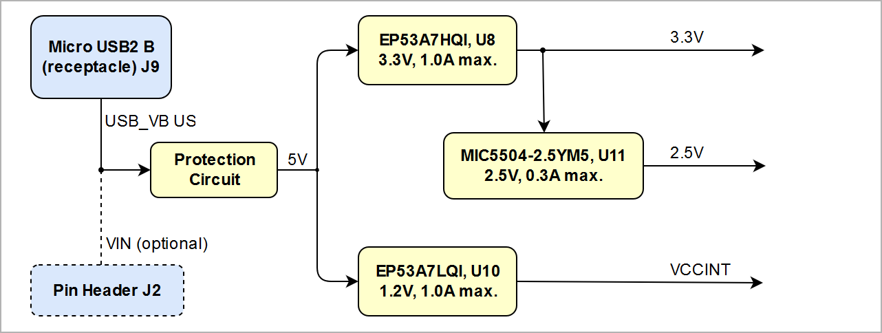
The FPGA module can be power-supplied through Micro USB2 connector J9 with supply voltage 'USB-VBUS' or alternative through pin header J2 with supply voltage 'VIN'.
The TEI0001 module needs one single power supply of 5.0V nominal.
There are following dependencies how the initial voltage of the extern power supply is distributed to the on-board DCDC converters:
|
| FPGA | Design | Typical Power, 25C ambient |
|---|---|---|
| Intel MAX 10 10M08 FPGA SoC | Not configured | TBD* |
Table 12: Module power consumption
*TBD - To Be Determined.
Actual power consumption depends on the FPGA design and ambient temperature.
There is no specific or special power-on sequence, just one single power source is needed.
| Connector Designator | VCC / VCCIO Schematic Name | Voltage | Direction | Pins | Notes |
|---|---|---|---|---|---|
| J2 | 5V | 5.0V | Out | Pin 14 | - |
| VIN | 5.0V | In | Pin 13 | - | |
| 3.3V | 3.3V | Out | Pin 12 | - | |
| J6 | 3.3V | 3.3V | Out | Pin 6, 12 | - |
| J9 | USB_VBUS | 5.0V | In | Pin 1 | - |
Table 13: Connector power pin description
Bank | Voltage | Voltage Range |
|---|---|---|
| 2 | 3.3V | all bank voltages fixed |
| 3 | 3.3V | |
| 5 | 3.3V | |
| 6 | 3.3V | |
| 1A | 3.3V | |
| 1B | 3.3V | |
| 8 | 3.3V |
Table 14: FPGA SoC VCCO bank voltages
Parameter | Min | Max | Units | Reference document |
|---|---|---|---|---|
VIN supply voltage (5.0V nominal) | -0.3 | 6.0 | V | EP53A7HQI datasheet |
| I/O Input voltage for FPGA I/O bank | -0.5 | 4.12 | V | Intel MAX 10 datasheet |
Storage Temperature | -40 | +90 | °C | LED R6C-AL1M2VY/3T datasheet |
Table 15: Absolute maximum ratings
| Parameter | Min | Max | Units | Reference document |
|---|---|---|---|---|
| VIN supply voltage (5.0V nominal) | 4.75 | 5.25 | V | same as USB-VBUS specification |
| I/O Input voltage for FPGA I/O bank | –0.5 | 3.6 | V | Intel MAX 10 datasheet |
| Operating temperature range | 0 | +70 | °C | Winbond datasheet W9864G6GT |
Table 16: Recommended operating conditions
| Please check Intel MAX 10 datasheet for complete list of absolute maximum and recommended operating ratings for the FPGA device. |
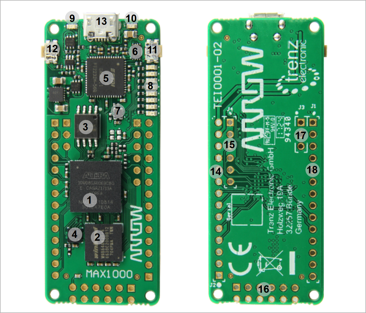
Board size: PCB 25mm × 61,5mm. Notice that some parts the are hanging slightly over the edge of the PCB like the the Micro USB2 B connector, which determine the total physical dimensions of the carrier board. Please download the assembly diagram for exact numbers.
PCB thickness: ca. 1.65mm
Highest part on the PCB without fitted headers and connectors is the Micro USB2 B connector, which has an approximately hight of 3 mm. Please download the step model for exact numbers.
|
| Date | Revision | Notes | PCN | Documentation Link |
|---|---|---|---|---|
| - | 03 | Current available revision | - | TEI0001-03 |
| - | 02 | First Production Release | - | TEI0001-02 |
| - | 01 | Prototypes | - | TEI0001-01 |
Table 17: Module hardware revision history
Hardware revision number is printed on the PCB board together with the module model number separated by the dash.
|
| Date | Revision | Contributors | Description |
|---|---|---|---|
| Ali Naseri |
| ||
2018-06-29 | v.17 | Ali Naseri |
|
Table 18: Document change history