Design Name always "TE Series Name" + optional CPLD Name + "CPLD"
|
Overview
Firmware for PCB CPLD with designator U2. CPLD Device in Chain: LCMX02-256HC
Feature Summary
Power Management
JTAG
Boot Mode
LED
- I2C
Firmware Revision and supported PCB Revision
See Document Change History
Product Specification
Port Description
Name / opt. VHD Name | Direction | Pin | Pullup/Down | Bank Power | Description |
|---|---|---|---|---|---|
BOOTMODE_1 | out | 21 | None | LVCMOS18 | Boot Mode Pin, connected to Zynq MIO5 (U1) |
EN_PL | out | 23 | Up | LVCMOS33 | Enable PL Power, connected to U4 |
F_TMS | out | 9 | Up | LVCMOS18 | JTAG chain to Zynq TMS (W11/U1), just pass through from TMS SLEWRATE=FAST DRIVE=8 |
F_TCK | out | 8 | Up | LVCMOS18 | JTAG chain to Zynq TCK (W12/U1), just pass through from TCK SLEWRATE=FAST DRIVE=8 |
F_TDI | out | 10 | Up | LVCMOS18 | JTAG chain to Zynq TDI (V11/U1), just pass through from TDI SLEWRATE=FAST DRIVE=8 |
F_TDO | in | 11 | None | LVCMOS18 | JTAG chain to Zynq TDO (W10/U1), just pass through from TDO, maxdelay 10ns |
I2C_SCL | in | 17 | None | LVCMOS18 | I2C Bus from SoC |
I2C_SDA | inout | 16 | None | LVCMOS18 | I2C Bus from SoC |
JTAG_EN | in | 26 | - | VCCIO 3.3 V | Enable JTAG access to CPLD for Firmware update (zero: JTAG routed to module, one: CPLD access) |
MIO0 | in | 14 | Up | LVCMOS18 | sd card detection signal coming from connected B2B, also connected to Zynq. Default: Only SD/QSPI Boot mode possible |
MIO8 | in | 13 | Up | LVCMOS18 | external pullup, for status of 'qspi_fbclk' from Zynq |
PS_SRST | in | 12 | Up | LVCMOS18 | system reset signal coming from connected B2B, also connected to Zynq. |
PWR_PL_OK | in | 27 | Up | LVCMOS33 | power good for PL |
PWR_PS_OK | in | 28 | Up | LVCMOS33 | power good for PS |
RST_IN_N | in | 25 | None | LVCMOS18 | Main Reset to U41 (PS_1.8V) coming from connected B2B |
RTC_INT | in | 4 | None | LVCMOS33 | RTC output interrupt signal |
BOOTMODE | in | 20 | None | LVCMOS18 | readable BOOTMODE from B2B J2-133 (MIO4) |
TMS | in | 29 | Up | LVCMOS33 | JTAG coming from connected B2B, maxdelay 10ns |
TCK | in | 30 | Up | LVCMOS33 | JTAG coming from connected B2B, maxdelay 10ns |
TDI | in | 32 | Up | LVCMOS33 | JTAG coming from connected B2B, maxdelay 10ns |
TDO | out | 1 | None | LVCMOS33 | JTAG coming from connected B2B |
LED | out | 5 | None | LVCMOS33 | used as status LED, connected to green LED (D1); SLEWRATE=SLOW |
Functional Description
JTAG
JTAG signals routed directly through the CPLD to FPGA. Access between the CPLD and FPGA is realised by JTAG_EN (logical one for CPLD, logical zero for FPGA) on B2B J1-148 (JTAG_EN).
Boot Mode
The adjustable Boot Mode is depending on programmed firmware.
Default (for Boot mode QSPI/SD):
BOOTMODE_1 is set constant to 1. Boot mode can be changed between QSPI or SD with B2B J2-133 Pin (BOOTMODE/ Zynq (MIO4)).
Boot mode | MIO5 (BOOTMODE_1 from CPLD) | MIO4 (BOOTMODE from B2B J2-133) |
|---|---|---|
QSPI | 1 | 0 |
SD | 1 | 1 |
Optional (for Boot mode QSPI/SD/JTAG):
BOOTMODE_1 depends on MIO0 (sd card detection) connected to B2B J2-137 Pin (SD card detection/ Zynq (MIO0))
- sd card detected --> SD/QSPI boot mode
- no sd card detected --> JTAG/NA boot mode
Boot mode | MIO5 (BOOTMODE_1 from CPLD) | MIO4 (BOOTMODE from B2B J2-133) | comments |
|---|---|---|---|
| JTAG | 0 | 0 | SD card is not allowed to be inserted |
| NAND | 0 | 1 | not supported boot mode! |
QSPI | 1 | 0 | inserted SD card is required |
SD | 1 | 1 | inserted SD card is required |
I2C interface
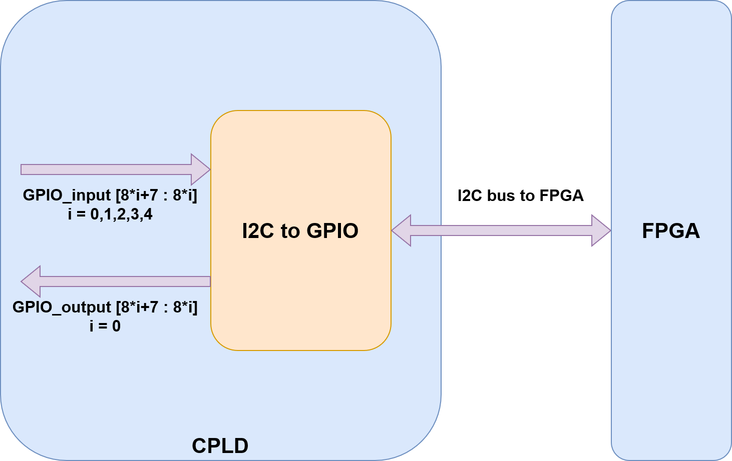
The CPLD firmware consists of an i2c-to-GPIO block. This subsystem provides an i2c protocol interface with several 8-bit registers (GPIO_input[8*i+7:8*i]) for reading from the CPLD as parallel general purpose inputs (I/Os). The read data is transferred to the FPGA via the i2c bus interface protocol. The chip address of this block in the firmware is 0x30, "i" is the data address in this case. The associated i2c bus is bus 1.
CPLD registers can be accessed via i2c interface in linux console with
- i2cget -y 1 0x30 <Index> (for reading) or
- i2cset -y 1 0x30 <Index> <Value> (for writing)
The following table shows the register map for the CPLD interface :
| Index | Byte | Register Name | Read/Write | Description | Default |
|---|---|---|---|---|---|
| 0x00 | [7:0] | USER_LED | R/W | User adjustable LED
| 0x01 |
| 0x01 | [7:0] | BOOTMODE_VAR | R | Bootmode variants (depending on firmware):
*no NAND flash present | 0x01 |
| 0x02 | [7:0] | CPLD_REVISION | R | CPLD revision | 0x03 |
| 0x03 | [7:0] | PCB_REVISION | R | PCB revision | 0x03 |
| 0x04 | [7:0] | STATUS_REGISTER | R | STATUS_REGISTER(4) = RTC_INT (Pin 4) | depending on BOOTMODE |
Power
PL Power is enabled.
LED
The green LED D1 can be set by the user via the I2C interface, as long as the module is not in error mode. In error mode, 4 different flashing sequences are currently implemented and prioritised. The lowest number has the highest priority.
| LED state | Priority | Description |
|---|---|---|
| Blink sequence *ooooooo | 1 | PWR_PS_OK not OK |
| Blink sequence **oooooo | 2 | PWR_PL_OK not OK |
| Blink sequence ***ooooo | 3 | Module is in reset state |
| Blink sequence ****oooo | 4 | BOOTMODE not OK
|
| USER LED | 5 | User adjustable LED (default is on) |
Appx. A: Change History and Legal Notices
Firmware Revision Changes
REV02 to REV03
- added input pin 'BOOMODE' to CPLD firmware (since REV03)
- added writing to I2C interface for user adjustable LED D1
- updated LED blinking sequence for error mode
- update readable I2C interface
REV01 to REV02
- added I2C interface
- defined generic parameter
- new Boot Mode variants (depending on firmware)
Document Change History
To get content of older revision go to "Change History" of this page and select older document revision number.
|
| Date | Document Revision | CPLD Firmware Revision | Supported PCB Revision | Authors | Description | Firmware release |
|---|---|---|---|---|---|---|
| REV03 | REV03 | REV03 documentation update | 2024-02-19 | |||
| 2023-02-07 | v.4 | REV02 | REV02, REV01 | Manuela Strücker | REV02 documentation update | 2023-02-07 |
| 2018-03-08 | v.3 | REV01 | REV01, REV02 | John Hartfiel | REV01 documentation update | 2016-05-30 |
| All |
Legal Notices
|
<style>
.wiki-content .columnLayout .cell.aside {
width: 20%;
}</style>
|
|