Design Name always "TE Series Name" + optional CPLD Name + "CPLD"
|
Overview
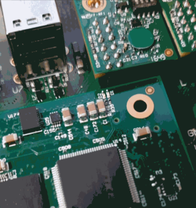
Firmware for PCB CPLD with designator U14. CPLD Device in Chain: LCMX02-1200HC
Feature Summary
Power Management
- Reset Management
Boot Mode
LED
- I2C
- UART
Firmware Revision and supported PCB Revision
See Document Change History
Product Specification
Port Description
| Name / opt. VHD Name | Direction | Pin | Pullup/Down | Bank Voltage | Description |
|---|---|---|---|---|---|
| BM0/MIO5 | out | 47 | None | LVCMOS33 | Boot Mode Pin |
| BM2/MIO4 | out | 48 | None | LVCMOS33 | Boot Mode Pin |
| BM3/MIO2 | out | 49 | None | LVCMOS33 | Boot Mode Pin |
| BOOTMODE | in | 99 | UP | LVCMOS33 | Boot Mode Pin from B2B / Used for UART as input to MIO9 |
| CONFIGX | out | 98 | UP | LVCMOS33 | MIO8 to B2B / Used for UART as output from MIO8 |
| CPLD_GPIO0 | 12 | - | - | / currently_not_used | |
| CPLD_GPIO1 | 11 | - | - | / currently_not_used | |
| CPLD_GPIO2 | 10 | - | - | / currently_not_used | |
| CPLD_GPIO3 | 9 | - | - | / currently_not_used | |
| CPLD_GPIO4 | 8 | - | - | / currently_not_used | |
| CPLD_GPIO5 | 7 | - | - | / currently_not_used | |
| CPLD_IO | 54 | - | - | / currently_not_used | |
| DONE | in | 34 | UP | LVCMOS33 | FPGA Done Pin |
| EN_1.0V_MGT / EN_1V0_MGT | out | 20 | None | LVCMOS33 | Power control |
| EN_1.2V_MGT / EN_1V2_MGT | out | 18 | None | LVCMOS33 | Power control |
| EN_1.8V | out | 16 | None | LVCMOS33 | Power control |
| EN_1V | out | 21 | None | LVCMOS33 | Power control |
| EN_3.3V | out | 15 | None | LVCMOS33 | Power control |
| ETH1_RESET | out | 53 | None | LVCMOS18 | ETH Reset |
| ETH1_RESET33 | in | 43 | UP | LVCMOS33 | ETH Reset from MIO7 |
| I2C_SCL | in | 58 | None | LVCMOS18 | I2C CLK / I2C CLK connected to module I2C interface |
| I2C_SDA | inout | 57 | None | LVCMOS18 | I2C DATA/ I2C SDA connected to module I2C interface |
| INIT | 36 | - | - | / currently_not_used | |
| JTAGENB | in | 82 | None | LVCMOS33 | Is used here to set bootmode JTAG(low) or QSPI(high) |
| LED1 / GLED | out | 4 | None | LVCMOS33 | green LED D2 |
| LED2 / RLED | out | 3 | None | LVCMOS33 | red LED D1 |
| M_TCK | in | 91 | None | LVCMOS33 | CPLD JTAG B2B |
| M_TDI | in | 94 | None | LVCMOS33 | CPLD JTAG B2B |
| M_TDO | out | 95 | None | LVCMOS33 | CPLD JTAG B2B |
| M_TMS | in | 90 | None | LVCMOS33 | CPLD JTAG B2B |
| MIO8 | in | 38 | UP | LVCMOS33 | used UART RS activity |
| MIO9 | out | 39 | None | LVCMOS33 | User IO, connected to BOOTMODE Pin on B2B |
| MMC_RST | out | 40 | None | LVCMOS33 | eMMC Reset |
| N.C. / dummy | 1 | - | - | / currently_not_used | |
| N.C. | 2 | - | - | / currently_not_used | |
| N.C. | 27 | - | - | / currently_not_used | |
| N.C. | 28 | - | - | / currently_not_used | |
| N.C. | 29 | - | - | / currently_not_used | |
| N.C. | 30 | - | - | / currently_not_used | |
| N.C. | 32 | - | - | / currently_not_used | |
| N.C. | 41 | - | - | / currently_not_used | |
| N.C. | 42 | - | - | / currently_not_used | |
| N.C. | 59 | - | - | / currently_not_used | |
| N.C. | 60 | - | - | / currently_not_used | |
| N.C. | 61 | - | - | / currently_not_used | |
| N.C. | 62 | - | - | / currently_not_used | |
| N.C. | 63 | - | - | / currently_not_used | |
| N.C. | 64 | - | - | / currently_not_used | |
| N.C. | 65 | - | - | / currently_not_used | |
| N.C. | 66 | - | - | / currently_not_used | |
| N.C. | 67 | - | - | / currently_not_used | |
| N.C. | 68 | - | - | / currently_not_used | |
| N.C. | 69 | - | - | / currently_not_used | |
| N.C. | 70 | - | - | / currently_not_used | |
| N.C. | 71 | - | - | / currently_not_used | |
| N.C. | 74 | - | - | / currently_not_used | |
| N.C. | 75 | - | - | / currently_not_used | |
| N.C. | 76 | - | - | / currently_not_used | |
| N.C. | 77 | - | - | / currently_not_used | |
| N.C. | 78 | - | - | / currently_not_used | |
| N.C. | 81 | - | - | / currently_not_used | |
| N.C. | 83 | - | - | / currently_not_used | |
| N.C. | 84 | - | - | / currently_not_used | |
| N.C. | 85 | - | - | / currently_not_used | |
| N.C. | 86 | - | - | / currently_not_used | |
| N.C. | 87 | - | - | / currently_not_used | |
| N.C. | 88 | - | - | / currently_not_used | |
| N.C. | 89 | - | - | / currently_not_used | |
| N.C. | 96 | - | - | / currently_not_used | |
| OTG-RST | out | 52 | UP | LVCMOS18 | OTG Rest |
| OTG-RST33 | in | 45 | UP | LVCMOS33 | OTG Reset from MIO0 |
| PG_1.0V_MGT | in | 19 | UP | LVCMOS33 | Power control |
| PG_1.2V_MGT | in | 17 | UP | LVCMOS33 | Power control |
| PG_1.8V | in | 14 | UP | LVCMOS33 | Power control |
| PG_1V | in | 25 | UP | LVCMOS33 | Power control |
| PG_1V5 | in | 24 | UP | LVCMOS33 | Power control |
| PG_3.3V | in | 13 | UP | LVCMOS33 | Power control |
| PROG_B | 35 | None | - | / currently_not_used | |
| PS_POR | out | 37 | None | LVCMOS33 | PS_POR_B (Power On Reset) |
| PS_SRST | out | 51 | None | LVCMOS18 | PS_SRST_B (PS Reset) |
| RESIN | in | 97 | UP | LVCMOS33 | Reset from B2B |
| RTC_INT | 31 | - | - | / currently_not_used |
Functional Description
JTAG
Used only for Firmware Update. Zynq has dedicated JTAG connection.
Power
Power enables (EN_1V, EN_1V8, EN_3V3, EN_1V2_MGT, EN_1V0_MGT) are all enabled sequentially.
EN_1V → EN_1V8 → EN_3V3 → EN_1V0_MGT → EN_1V2_MGT
Power goods (PG_1V, PG_1V5, PG_1V8, PG_3V3, PG_1V2_MGT, PG_1V0_MGT) are used for System Reset and LED Monitoring.
Boot Mode
JTAG or QSPI.
Bootmode is read through JTAGEN signal (can be set by DIP switch on carrier).
Can also be changed through software I2C after linux has bootet. (command: i2cset -y 0 0x20 0x03 <0x02 or 0x00>)
Reset
PS_POR is triggered by soft_resetn when bootmode is changed by software (I2C interface) or main power failed
PS_SRST is triggered when user reset pressed (RESIN) or main power failed.
ETH1_RESET is triggered when ETH1_RESET33(e.g. by fsbl) or main power failed.
OTG_RST is triggered when ETH1_OTG_RST33(e.g. by fsbl) or main power failed.
MMC_RST is triggered when main power failed.
main power failed - is triggered when at least one of the Power Good signals of the DCDCs goes down. |
UART
MIO8 is connected to CONFIGX. UART TX from FPGA to RX XMOD.
BOOTMODE is connected to MIO9. UART RX.
LED
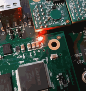
Red LED D1
| Blink sequence | Priority | Condition | Description |
|---|---|---|---|
******** | highest | RESIN = LOW (low active) | external reset "RESIN" is pressed |
| *******o | blink sequence not used | ||
| ******oo | blink sequence not used | ||
| *****ooo | PG_1V or PG_1V5 or PG_1V8 or PG_3V3 is zero | One of the Power Good Signals of internal Voltages DCDCs LOW | |
| ****oooo | blink sequence not used | ||
| ***ooooo | blink sequence not used | ||
| **oooooo | PG_1V2_MGT or PG_1V0_MGT is zero | One of the Power Good Signals of MGT Voltages DCDCs LOW | |
*ooooooo | DONE = '0' | FPGA not programmed, wrong Bootmode? Check JTAGEN signal. No design on QSPI Flash? | |
| continuously ON | lowest | software controlled command: i2cset -y 0 0x20 0x05 <0x00 or 0x01> | If none of the above condition is met |
Green LED D2
| Blink sequence | Priority | Condition | Description |
|---|---|---|---|
******** | highest | PG_1V or PG_1V5 or PG_1V8 or PG_3V3 or PG_1V2_MGT or PG_1V0_MGT is zero | Power Good Signal of DCDCs deassertion occurred after power up. Look at content of power good register → i2cget -y 0 0x20 0x02 |
| *******o | blink sequence not used | ||
| ******oo | blink sequence not used | ||
| *****ooo | blink sequence not used | ||
| ****oooo | blink sequence not used | ||
| ***ooooo | bootmode was changed via I2C. | command: i2cset -y 0 0x20 0x03 <0x02 or 0x00> | |
| **oooooo | blink sequence not used | ||
*ooooooo | blink sequence not used | ||
| UART activity | lowest | LED = MIO8 | If none of the above condition is met |
I2C Interface
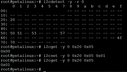
This subsystem provides 2 x 32-bit (8 x 8-bit) of general purpose parallel input and output (I/O) expansion for the I2C bus protocol. Address of this module is 0x20. This module contains eight 8-bit registers for reading and writing (GPIO_register_1[7:0] to GPIO_register_1[31:24] and GPIO_register_2[7:0] to GPIO_register_2[31:24]) separately with address 0x00 to 0x07. These registers can be accessed with I2C commands in linux console or with i2c functions in FSBL code. To access these registers the following commands in linux console can be used:
To see the i2c bus addresses : i2cdetect -y -r 0
To read register of i2c to GPIO module: i2cget -y 0 0x20 <register address>
To write data in a register of i2c to GPIO module: i2cset -y 0 0x20 <register address> <data>
|
All eight registers can be read, but only two of them can be written from the linux console.
| I2C Register | permissions | address | function | I2C command |
|---|---|---|---|---|
| GPIO_register_1(7 downto 0) | readable | 0x00 | contains the CPLD Firmware Revision (not the PCB revision) | read: i2cget -y 0 0x20 0x00 |
| GPIO_register_1(15 downto 8) | readable | 0x01 | contains the bootmode in bit 8 and bit 9. This register is read by the fsbl and printed in the console as the bootmode during power up | |
| GPIO_register_1(23 downto 16) | readable | 0x02 | Bit 17 to 23 contain the DCDC power good signals and the DONE pin | |
| GPIO_register_1(31 downto 24) | readable/writeable | 0x03 | Bit 24 and 25 contain the bootmode, JTAG(b 00) or QSPI(b 10) | write: i2cset -y 0 0x20 0x03 <0x02 or 0x00> |
| GPIO_register_2(7 downto 0) | readable | 0x04 | Bit 0 to 3 show the state of the reset signals PS_POR, PS_SRST, ETH1_RESET, OTG_RST | |
| GPIO_register_2(15 downto 8) | readable/writeable | 0x05 | Bit 8 can be controlled to change the state of the red LED D1 if no other red LED condition is met | write: i2cset -y 0 0x20 0x05 <0x00 or 0x01> |
| GPIO_register_2(23 downto 16) | readable | 0x06 | not used | |
| GPIO_register_2(31 downto 24) | readable | 0x07 | not used |
Appx. A: Change History and Legal Notices
Revision Changes
Document Change History
To get content of older revision got to "Change History" of this page and select older document revision number.
|
| Date | Document Revision | CPLD Firmware Revision | Supported PCB Revision | Authors | Description | Firmware release |
|---|---|---|---|---|---|---|
| REV02 | REV02 |
| Revision 02, 28.11.2023 released | |||
2018-05-25 | v.5 | REV01 | RE02 | John Hartfiel
|
| |
| v.3 | REV01 | RE02 | John Hartfiel |
| ||
| 2018-03-12 | v.1 |
| ||||
| All |
Legal Notices
|
<style>
.wiki-content .columnLayout .cell.aside {
width: 20%;
}</style>
|
|


