<!-- Template Revision 1.2 --> |
Online version of this manual and other related documents can be found at https://wiki.trenz-electronic.de/display/IP/Trenz+Electronic+IP+Cores |
Table of Contents |
| ||||||||||||||||||||||||||||||||||||||||||
This Trenz Electronic teCORE IP provides a RGPIO (Remote GPIO) Interface to talk to external RGPIO Devices over 3 wire
IP can be used as Master communicate with external RGPIO devices with Slave interface or as Slave communicate with external RGPIO devices with Master interface
This Trenz Electronic teCORE is licensed under MIT License. This IP is included in various Reference Designs or contact Trenz Electronic Support (support[at]trenz-electronic.de) with subject line "[TE-IP-Core Request]" to order this IP-Core.
Maximum RGPIO output CLK depends on Master and Slave device implementation. In the most cases maximum frequency of 25MHz is allowed.
Communication channel between master and slave interface.
| Port Name | IO | Description |
|---|---|---|
| RGPIO_M_CLK | out | RGPIO Master Clock |
| RGPIO_M_RX | in | RGPIO Master RXD |
| RGPIO_M_TX | out | RGPIO Master TXD |
| Port Name | IO | Description |
|---|---|---|
| RGPIO_S_CLK | out | RGPIO Slave Clock |
| RGPIO_S_RX | in | RGPIO Slave RXD |
| RGPIO_S_TX | out | RGPIO Slave TXD |
Master user interface to communicate with slave device.
| Port Name | IO | Description |
|---|---|---|
| RGPIO_M_OUT | out | 23bit data output to slave device* |
| RGPIO_M_IN | in | 23bit data input from slave device* |
| RGPIO_M_RESERVED_OUT | out | 4bit reserved for future usage |
| RGPIO_M_RESERVED_IN | in | 4bit reserved for future usage |
| RGPIO_M_SLAVE_ACTIVATION_CODE | out | 4bit activation code from external slave for information only |
| RGPIO_M_ENABLE | in | Enable RGPIO communication. High active. Set RGPIO data as valid for Slave. Data will always transmitted, if CLK is available. |
| RGPIO_M_USRCLK | in | RGPIO transmission CLK for master and slave |
| RGPIO_M_RESET_N | in | RGPIO Reset. Low active. |
*currently limited to 23 bit to use IP with CPLD implementations of TE Boards. For general usage, this restriction will be removed on future IP update.
Slave user interface to communicate with master device.
| Port Name | IO | Description |
|---|---|---|
| RGPIO_S_OUT | out | 23bit data output to master device* |
| RGPIO_S_IN | in | 23bit data input from master device* |
| RGPIO_S_RESERVED_OUT | out | 4bit reserved for future usage |
| RGPIO_S_RESERVED_IN | in | 4bit reserved for future usage |
| RGPIO_S_MASTER_ACTIVATION_CODE | out | 4bit activation code from external master for information only |
| RGPIO_S_ENABLED | out | Interface status. Indicates RGPIO data are valid. |
*currently limited to 23 bit to use IP with CPLD implementations of TE Boards. For general usage, this restriction will be removed on future IP update.
This chapter includes guidelines and additional information to facilitate designing with the core.
This chapter describes customizing and generating the core, constraining the core, and the simulation, synthesis and implementation steps that are specific to this IP core. More detailed information about the standard Vivado® design flows and the Vivado IP integrator can be found in the following Vivado Design Suite user guides:
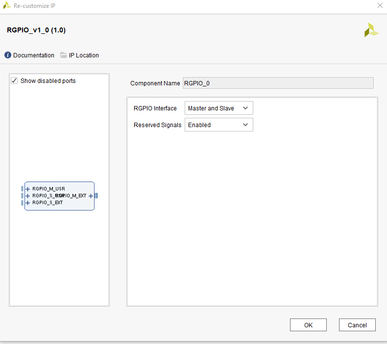
This section includes information about using Xilinx® tools to customize and generate the core in the Vivado Design Suite.

This section contains information about constraining the core in the Vivado Design Suite.
Loc constrains and IO Standard depends on module and usage.
This section is not applicable for this IP core.
Maximum RGPIO output CLK depends on Master and Slave device implementation. In the most cases maximum frequency of 25MHz is always allowed.
This section is not applicable for this IP core.
This section is not applicable for this IP core.
This section is not applicable for this IP core.
This section is not applicable for this IP core.
This section is not applicable for this IP core.
This core does not support simulation.
This section contains information about synthesis and implementation in the Vivado Design Suite. For details about synthesis and implementation, see the Vivado Design Suite User Guide:
There is no example Design for this IP core release.
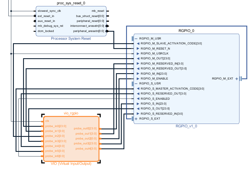
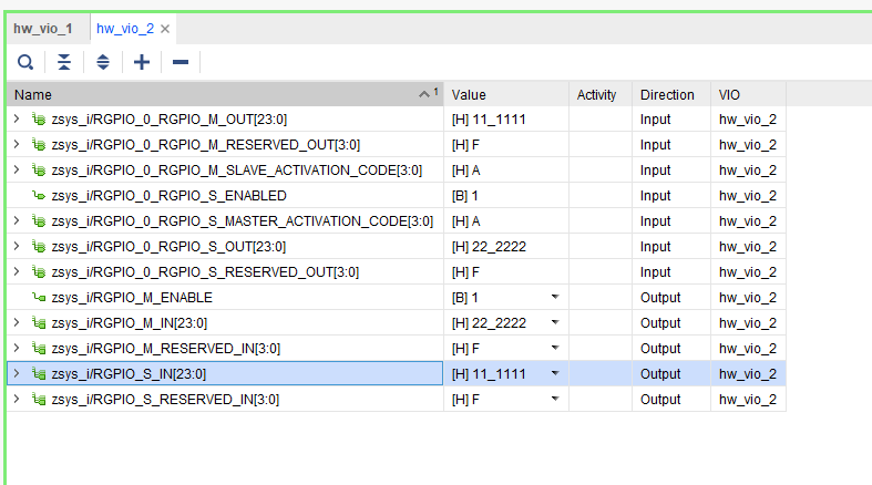
Use Master Slave loopback over RGPIO_EXT interface to test IP Master and Slave Interface together.
Vivado Block Design:

VIO HW Manager:

There is no test bench for this IP core release.
| Date | Document Revision | IP Revision | Authors | Description |
|---|---|---|---|---|
| v1.0 |
|