Table of Contents
Download PDF version of this document. |
Table of Contents |
Refer to https://wiki.trenz-electronic.de/display/PD/TE0713+TRM for the online version of this manual and the rest of available documentation. |
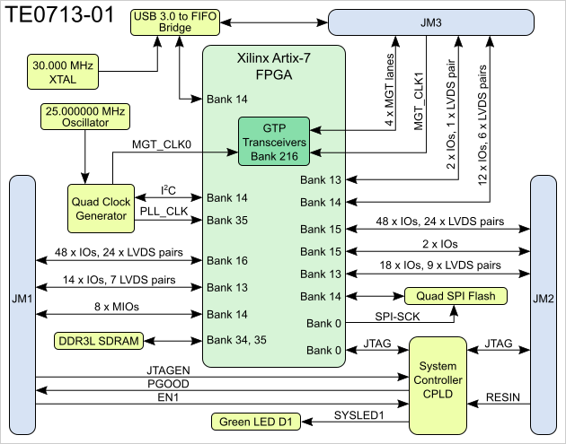
Trenz Electronic TE0713 is an industrial-grade FPGA module integrating Xilinx Artix-7 FPGA, USB 3.0 to FIFO bridge, 1 GByte of DDR3L SDRAM, 32 MByte Flash memory for configuration and operation, and powerful switching-mode power supplies for all on-board voltages. Numerous configurable I/Os are provided via rugged high-speed strips. All this on a tiny footprint, smaller than a credit card size at very competitive price. All Trenz Electronic SoMs in 4 x 5 cm form factor are mechanically compatible.
Evenly-spread supply pins for good signal integrity
Additional assembly options are available for cost or performance optimization upon request.
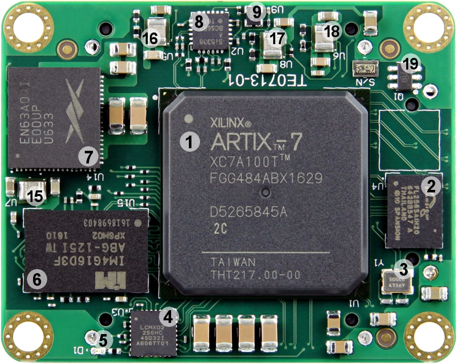
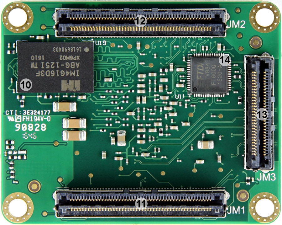
Programmable unit | Content | Notes |
|---|---|---|
| Xilinx Artix-7 FPGA | Not programmed | U1 |
| System Controller CPLD | Programmed | U3 |
| SPI Flash OTP area | Empty | U4 |
SPI Flash main array | Empty | U4 |
| SPI Flash Quad Enable bit | Set | U4 |
FPGA banks and I/O signals connected to the B2B connectors:
| FPGA Bank | B2B Connector | I/O Signal Count | Voltage Level | Notes |
|---|---|---|---|---|
| 13 | JM1 | 14 | VCCIO13 | Supplied by the baseboard. |
| 13 | JM2 | 18 | VCCIO13 | Supplied by the baseboard. |
| 13 | JM3 | 2 | VCCIO13 | Supplied by the baseboard. |
| 14 | JM1 | 8 | 3.3V | |
| 14 | JM3 | 12 | 3.3V | |
| 15 | JM2 | 48 | VCCIO15 | Supplied by the baseboard. |
| 15 | JM2 | 2 | VCCIO15 | Supplied by the baseboard. |
| 16 | JM1 | 48 | VCCIO16 | Supplied by the baseboard. |
JTAG access to the Xilinx Artix-7 FPGA and System Controller CPLD devices is provided through B2B connector JM2.
JTAG Signal | B2B Pin |
|---|---|
| TMS | JM2-93 |
| TDI | JM2-95 |
| TDO | JM2-97 |
| TCK | JM2-99 |
JTAGEN pin in B2B connector JM1 is used to select JTAG access for FPGA or System Controller CPLD:
| JTAGEN | JTAG Access To |
|---|---|
| Low | Artix-7 FPGA |
| High | System Controller CPLD |
Special purpose pins are connected to System Controller CPLD and have following default configuration:
| Pin Name | Mode | Function | Default Configuration |
|---|---|---|---|
| PGOOD | Output | Power good | Active high when all on-module power supplies are working properly. |
| JTAGEN | Input | JTAG select | Low for normal operation, high for System Controller CPLD access. |
| EN1 | Input | Power Enable | When forced low, pulls POR_B low to emulate power on reset. |
| NOSEQ | - | No function | Not used. |
| MODE | - | No function | Not used. |
The TE0713-01 module has one LED which is connected to the System Controller CPLD. Once FPGA configuration has completed, it can be used by the user's design.
| LED | Color | SC Signal | SC Pin | Notes |
|---|---|---|---|---|
| D1 | Green | SYSLED1 | 8 | Exact function is defined by SC CPLD firmware. |
On-board Si5338 clock generator chip is used to generate clocks with 25 MHz oscillator connected to the pin IN3 as input reference. There is a I2C bus connection between the FPGA bank 14 (master) and clock generator chip (slave) which can be used to program output frequencies. See the reference design for more information.
| CLK Output | FPGA Bank | FPGA Pin | IO Standard | Net Name | Default Freq | Note |
|---|---|---|---|---|---|---|
| CLK0 | - | - | - | - | -- | N.C. |
| CLK1 | - | - | - | - | -- | N.C. |
| CLK2 | 216 | F6/E6 | Auto | MGT_CLK0_P/N | 125 MHz | GTP transceiver clock. |
| CLK3 | 35 | H4/G4 | LVDS | PLL_CLK_P/N | 200 MHz | AC coupled, board termination |
On-board QSPI flash memory S25FL256S (U14) is used to store initial FPGA configuration. Besides FPGA configuration, remaining free flash memory can be used for user application and data storage. All four SPI data lines are connected to the FPGA allowing x1, x2 or x4 data bus widths. Maximum data rate depends on the selected bus width and clock frequency used.
SPI Flash QE (Quad Enable) bit must be set to high or FPGA is unable to load its configuration from flash during power-on. By default this bit is set to high at the manufacturing plant. |
System Controller CPLD (Lattice Semiconductor MachXO2-256HC, U3) is used to control FPGA configuration process. The FPGA is held in reset (by driving the PROG_B signal low) until all power supplies have stabilized.
By driving signal RESIN to low you can reset the FPGA. This signal can be driven from the user’s baseboard PCB via the B2B connector JM2 pin 18.
Input EN1 is also gated to FPGA reset, should be open or pulled up for normal operation. By driving EN1 low, on-board DC-DC converters will be not turned off.
User can create their own System Controller design using Lattice Diamond software. Once created it can be programmed into CPLD via JTAG interface.
The TE0713-01 SoM has two 4 Gbit volatile DDR3 SDRAM ICs (U15 and U19) for storing user application code and data.
Configuration of the DDR3 memory controller in the FPGA should be done using the MIG tool in the Xilinx Vivado Design Suite IP catalog.
TE0713-01 is equipped with the FTDI FT600Q high performance USB 3.0-to-FIFO interface bridge chip.
Single 3.3V power supply (for both VIN and 3.3VIN power rails) with minimum current capability of 3A for system startup is recommended.
Power Consumption
Typical module power consumption is between 2-3W. Exact power consumption is to be determined.
TE0713-01 module can also be powered by split 5V/3.3V power sources if preferred. In such case apply 5V to B2B connectors VIN pins and 3.3V to 3.3VIN pins, although lowest power consumption is achieved when powering the module from single 3.3V supply. When using split 5V/3.3V supplies the power consumption (and heat dissipation) will rise due to the DC-DC converter efficiency (it decreases when VIN/VOUT ratio rises).
For the highest efficiency of the on-board DC-DC regulators, it is recommended to use same 3.3V power source for both VIN and 3.3VIN power rails. Although VIN and 3.3VIN can be powered up in any order, it is recommended to power them up simultaneously.
It is important that all baseboard I/Os are 3-stated at power-on until System Controller sets PGOOD signal high (B2B connector JM1, pin 30), or 3.3V is present on B2B connector JM2 pins 10 and 12, meaning that all on-module voltages have become stable and module is properly powered up.
See Xilinx datasheet DS181 - "Artix-7 FPGAs Data Sheet: DC and AC Switching Characteristics" for additional information. User should also check related baseboard documentation when choosing baseboard design for TE0713 module.
Power Rail Name | B2B Connector JM1 Pin | B2B Connector JM2 Pin | Direction | Notes |
|---|---|---|---|---|
VIN | 1, 3, 5 | 2, 4, 6, 8 | Input | SoM supply voltage (from the baseboard). |
| 3.3VIN | 13, 15 | - | Input | SoM supply voltage (from the baseboard). |
| DDR_PWR | - | 19 | Output | Module internal supply of 1.35V level. |
| 1V | - | - | - | Module internal supply of 1V level. |
| 1V_MGT | - | - | - | Module internal supply of 1V for bank 216 transceivers. |
| 1.2V_MGT | - | - | - | Module internal supply of 1.2V for bank 216 transceivers. |
1.8V | 39 | - | Output | Module internal 1.8V level. Maximum 300mA available. |
| 3.3V | - | 10, 12 | Output | Module internal 3.3V level. |
| VCCIO13 | - | 1, 3 | Input | High-Range bank supply voltage (from the baseboard). |
| VCCIO15 | - | 7, 9 | Input | High-Range bank supply voltage (from the baseboard). |
| VCCIO16 | 9, 11 | - | Input | High-Range bank supply voltage (from the baseboard). |
| VREF_JTAG | - | 91 | Output | JTAG reference voltage (3.3V). |
Module Variant | FPGA | Junction Temperature | Temperature Range |
|---|---|---|---|
| TE0713-01-100-2C | XC7A100T-2FGG484C | 0°C to 85°C | Commercial grade |
| TE0713-01-200-2C | XC7A200T-2FBG484C | 0°C to 85°C | Commercial grade |
Parameter | Min | Max | Units | Reference Document |
|---|---|---|---|---|
VIN supply voltage | -0.3 | 7.0 | V | See EN63A0QI and TPS82085 datasheets. |
| 3.3VIN supply voltage | -0.5 | 3.75 | V | See LCMXO2-256HC datasheet. |
| HR I/O banks supply voltage (VCCO) | -0.5 | 3.6 | V | Xilinx datasheet DS181 |
| HR I/O banks input voltage | -0.4 | VCCO + 0.55 | V | Xilinx datasheet DS181 |
| GTP transceivers Tx/Rx input voltage | -0.5 | 1.26 | V | Xilinx datasheet DS181 |
Storage temperature | -55 | 100 | °C | See IM4G16D3FABG datasheet. |
| Parameter | Min | Max | Units | Reference Document |
|---|---|---|---|---|
| VIN supply voltage | 2.5 | 6.0 | V | See TPS82085 datasheet. |
| 3.3VIN supply voltage | 2.375 | 3.6 | V | See LCMXO2-256HC datasheet. |
| HR I/O banks supply voltage (VCCO) | 1.14 | 3.465 | V | Xilinx datasheet DS181 |
| HR I/O banks input voltage | -0.20 | VCCO + 0.2 | V | Xilinx datasheet DS181 |
Commercial grade: 0°C to +70°C.
Industrial grade: -40°C to +85°C.
Operating temperature range depends also on customer design and cooling solution. Please contact us for options.
| Assembly variants for higher storage temperature range are available on request. |
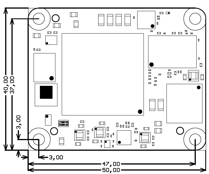
All dimensions are shown in millimeters.
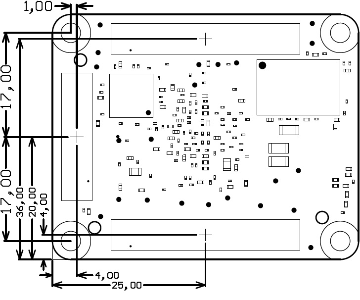
21 g Plain module.
8.8 g Set of nuts and bolts.
| Date | Revision | Notes | PCN | Documentation Link |
|---|---|---|---|---|
| 2016-06-30 | 01 | First production revision | TE0713-01 |
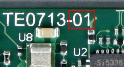
Hardware revision number is printed on the PCB board together with the module model number separated by the dash.
Date | Revision | Contributors | Description |
|---|---|---|---|
| John Hartfiel |
| ||
| v.8 | John Hartfiel |
| |
| 2017-05-28 | v.6 | Jan Kumann |
|
| 2017-02-07 | v.1 | Jan Kumann |
|