Template Revision 2.7
- Module: TRM Name always "TE Series Name" +TRM
Example: "TE0728 TRM" - Carrier: TRM Name usually "TEB Series Name" +TRM
Example: "TEB0728 TRM"
|
<!-- tables have all same width (web max 1200px and pdf full page(640px), flexible width or fix width on menu for single column can be used as before) -->
<style>
.wrapped{
  width: 100% !important;
  max-width: 1200px !important;
 }
</style> |
----------------------------------------------------------------------- |
Note for Download Link of the Scroll ignore macro: |
Table of Contents 
|
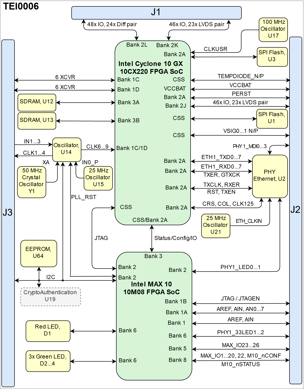
Overview
The Trenz Electronic TEI0006 is an industrial grade module based on Intel® Cyclone 10 GX. Intel® Cyclone 10 GX device family delivers higher core, transceiver, and I/O performance than the previous generation of low cost FPGAs.
Refer to http://trenz.org/tei0006-info for the current online version of this manual and other available documentation.
Key Features
Block Diagram
Main Components
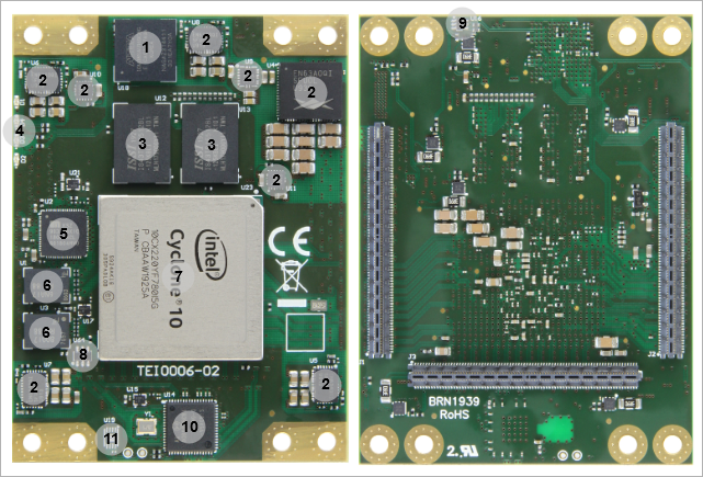
Notes : - Picture of the PCB (top and bottom side) with labels of important components
- Add List below
|
- Intel® MAX 10, U18
- DC/DC convertor, U4...11
- SDRAM DDR3 Memory, U12 - U13
- User LEDs, D1...4
- Ethernet Transceiver, U2
- SPI Flash Memory, U1 - U3
- Intel® Cyclone 10 GX, U23
- EEPROM, U64
- Buffer, U16
- 10-Channel Clock Multiplier, U14
- CryptoAuthentication Device (optional), U19
Initial Delivery State
Notes : Only components like EEPROM, QSPI flash and DDR3 can be initialized by default at manufacture. If there is no components which might have initial data ( possible on carrier) you must keep the table empty |

Storage device name | Content | Notes |
|---|
| Intel® MAX 10 | Programmed | See CPLD Firmware | Quad SPI Flash | Not Programmed |
| | EEPROM | Programmed | Ethernet MAC | | DDR3 SDRAM | Not Programmed |
|
|
Configuration Signals
- Overview of Boot Mode, Reset, Enables.
|
The TEI0006 module can be configured using different modes. Mode selection can be done using MSEL[2:0]. MSEL2 is connected to GND so mode selection can be done using MSEL[1:0] which are connected to Bank 3 of Intel Max 10.
MODE Signal State | MSEL2 | MSEL1 | MSEL0 | Boot Mode |
|---|
MSEL[2:0] | 0 | 1 | 0 | AS / Fast | | 0 | 1 | 1 | AS / Standard | | 0 | 0 | 0 | PS and FPP / Fast | | 0 | 0 | 1 | PS and FPP / Standard |
|
By tying the CONF_DONE, NSTATUS, and NCONFIG pins together, the devices initialize and enter user mode at the same time. If any device in the chain detects an error, configuration stops for the entire chain and you must reconfigure all the devices. For example, if the first device in the chain flags an error on the NSTATUS pin, it resets the chain by pulling its NSTATUS pin low.
| Signals | Connected to | Description | Note |
|---|
| NCONFIG | 1.8V | Configuration trigger | From U18 (Intel MAX 10) - Bank 3 | | CONF_DONE | 1.8V | Configuration done | To U18 (Intel MAX 10) - Bank 3 | | NSTATUS | 1.8V | Configuration status | To U18 (Intel MAX 10) - Bank 3 | | DCLK | U1 | Configuration clock | To U1 (Flash Memory) From U18 (Intel MAX 10) - Bank 3 | | AS_DATA0...3 | U1 | Configuration data | From U1 (Flash Memory) |
|
Signal | B2B | Connected to | Note |
|---|
PERST | J2-99 | Bank A2 |
|
|
Signals, Interfaces and Pins
Notes : - For carrier or stand-alone boards use subsection for every connector type (add designator on description, not on the subsection title), for example:
- For modules which needs carrier use only classes and refer to B2B connector if more than one is used, for example
|
Board to Board (B2B) I/Os
FPGA bank number and number of I/O signals connected to the B2B connector:
| FPGA | FPGA Bank | B2B Connector | I/O Signal Count | Voltage Level | Notes |
|---|
Intel Cyclone 10 GX | Bank 1C | J3 | 12 Diff pair | 0.95V | GXBL1C_RX0...5 N/P, GXBL1C_TX0...5 N/P | Bank 1D | J3 | 12 Diff pair | 0.95V | GXBL1D_RX0...5 N/P, GXBL1D_TX0...5 N/P | Bank 2A | J2 | 2 Single ended | 1.8V | PERST, CLKUSR | Bank 2J | J2 | 46 Single ended (23 Diff pair) | VCCIO2J |
| Bank 2K | J1 | 46 Single ended (23 Diff pair) | VCCIO2K |
| Bank 2L | J1 | 48 Single ended (24 Diff pair) | VADJ up to 3 V |
| Bank 3A | - | - | 1.35V | VDD_DDR | Bank 3B | - | - | 1.35V | VDD_DDR | Intel Max 10 | Bank 1A | J2 | 8 Single ended | 3.3V |
| Bank 1B | J2 | 5 Single ended | 3.3V |
| Bank 2 | J3 | 1 Single ended | 1.8VIO |
| Bank 3 | - | - | 1.8VIO |
| Bank 5 | J2 | 3 Single ended | 3.3V |
| Bank 6 | J2 | 2 Single ended | 3.3V |
| Bank 8 | J2 | 23 Single ended | 3.3V |
|
|
JTAG Interface
JTAG access to the TEI0006 SoM is through B2B connector J2. JTAGEN is pulled up to 3.3V and after power on, JTAG for MAX 10 CPLD is enabled. JTAG port of Cyclon 10 GX device is routed to MAX10 CPLD IOs. The default Firmware connects the JTAG port of the Cyclon 10 GX to the IO pins of the JTAG port in user IO mode. Setting JTAGEN to GND enables JTAG for the Cyclon 10 GX device.
JTAG Signal | B2B Connector | Note |
|---|
| TMS | J2-160 |
| | TDI | J2-159 |
| | TDO | J2-158 |
| | TCK | J2-157 |
| | JTAGEN | J2-105 | Pulled up to 3.3V. |
|
MIO Pins
you must fill the table below with group of MIOs which are connected to a specific components or peripherals, you do not have to specify pins in B2B, Just mention which B2B is connected to MIOs. The rest is clear in the Schematic. Example: | MIO Pin | Connected to | B2B | Notes |
|---|
| MIO12...14 | SPI_CS , SPI_DQ0... SPI_DQ3 SPI_SCK | J2 | QSPI |
|
| MIO Pin | Connected to | B2B | Notes |
|---|
| MAX_IO1...20, 22 | U18 (Intel MAX 10) - Bank 8 | J2 |
| | MAX_IO23, 25, 26 | U18 (Intel MAX 10) - Bank 5
| J2 |
|
|
On-board Peripherals
Notes : - add subsection for every component which is important for design, for example:
- Two 100 Mbit Ethernet Transciever PHY
- USB PHY
- Programmable Clock Generator
- Oscillators
- eMMCs
- RTC
- FTDI
- ...
- DIP-Switches
- Buttons
- LEDs
|
Notes : In the on-board peripheral table "chip/Interface" must be linked to the corresponding chapter or subsection |
QSPI Flash Memory
Notes : Minimum and Maximum density of quad SPI flash must be mentioned for other assembly options. |
The TEI0006 is equipped with two Micron SPI flash memory. On-board SPI flash memory is used to store initial FPGA configuration. Besides FPGA configuration, remaining free flash memory can be used for user application and data storage. All four SPI data lines are connected to the FPGA allowing x1 or x4 data bus widths. Maximum data rate depends on the selected bus width and clock frequency.
| Designator | Schematic | Connected to | Notes |
|---|
U1
| NCSO | CSS Bank (Configuration Bank) | Used when you are not configuring using AS | | DCK | DCLK | AS Configuration Clock | | AS_DATA0 | CSS Bank (Configuration Bank) |
| | AS_DATA1 | CSS Bank (Configuration Bank) |
| | AS_DATA2 | CSS Bank (Configuration Bank) |
| | AS_DATA3 | CSS Bank (Configuration Bank) |
| | U3 | QSPI_CS | Bank 2A |
| | QSPI_CK | Bank 2A |
| | QSPI_DATA0 | Bank 2A |
| | QSPI_DATA1 | Bank 2A |
| | QSPI_DATA2 | Bank 2A |
| | QSPI_DATA3 | Bank 2A |
|
|
EEPROM
| Schematic | U64 EEPROM Pin | B2B | U18 Intel Max 10 Pin | Notes |
|---|
| I2C_SCL | SCL | J3-135 | Bank 2 - K2 |
| | I2C_SDA | SDA | J3-137 | Bank 2 - L2 |
|
|
| Pins | I2C Address | Designator | Notes |
|---|
| I2C_SCL, I2C_SDA | 0x53 | U64 |
|
|
DDR3 SDRAM
Notes : Minimum and Maximum density of DDR3 SDRAM must be mentioned for other assembly options. (pay attention to supported address length for DDR3) |
The TEI0006 SoM has two 1 GByte volatile DDR3 SDRAM IC provided by Integrated Silicon Solution Inc for storing user application code and data.
- Part number: IS43TR16512BL
- Supply voltage: 1.35 V
- Speed: Half rate: 533 MHz; Quarter rate: max. 800 MHz
- Temperature: -40 °C to 95 °C
Ethernet PHY
| Signal Name | Connected to | B2B | Signal Description |
|---|
PHY1_MDI0_P PHY1_MDI0_N | - - | J2-93 J2-91 |
| PHY1_MDI1_P PHY1_MDI1_N | - - | J2-87 J2-85 |
| PHY1_MDI2_P PHY1_MDI2_N | - - | J2-81 J2-79 |
| PHY1_MDI3_P PHY1_MDI3_N | - - | J2-75 J2-73 |
| | ETH1_RST | U23, Bank 2A | - | Pulled-up to DVDDH Voltage. | | ETH1_MDC | U23, Bank 2A | - | Pulled-up to DVDDH Voltage. | | ETH1_MDIO | U23, Bank 2A | - | Pulled-up to DVDDH Voltage. | | ETH1_TXD0...7 | U23, Bank 2A | - | 8 bit Transfer | | ETH1_RXD0...7 | U23, Bank 2A | - | 8 bit Receive | | ETH1_GTXCK | U23, Bank 2A | - |
| | ETH1_TXCLK | U23, Bank 2A | - |
| | ETH1_TXEN | U23, Bank 2A | - |
| | ETH1_TXER | U23, Bank 2A | - |
| | ETH1_RXCK | U23, Bank 2A | - | Pulled-down to GND. | | ETH1_RXDV | U23, Bank 2A | - | Pulled-down to GND. | | PHY1_INT | - | - | Pulled-up to DVDDH Voltage. | | PHY1_LED1 | U18, Bank 2 | - | Pulled-up to DVDDH Voltage. | | PHY1_LED2 | U18, Bank 2 | - | Pulled-down to GND. | | ETH1_CRS | U23, Bank 2A | - |
| | ETH1_XTAL_IN | ETH_CLKIN | - | From U21 (25 MHz Oscillator) |
|
Intel MAX 10
The TEI0006 is equipped with an Intel MAX 10 device which is a single-chip, non-volatile low-cost programmable logic device (PLD) to integrate the optimal set of system components. Intel MAX 10 (U18) is power and configuration controller on TEI0006 SoM.
| Intel Max 10 Bank | Signals | Connected to | Description | Notes |
|---|
| Bank 1A | AIN0...7 | B2B- J2 |
|
| | Bank 1B | TCK, TDO, TMS, TDI, JTAGEN | B2B- J2 |
|
| | Bank 2 | PHY1_LED1 PHY1_LED2 | Ethernet PHY, U2 Ethernet PHY, U2 | Ethernet LED Ethernet LED | Pulled-up to DVDDH. Pulled-down to GND. | | F_TCK, F_TDO, F_TDI, F_TMS | Intel Cyclone 10 GX (U23) - Bank CSS | Intel Cyclone 10 JTAG signals |
| | I2C_SDA, I2C_SCL | EEPROM, U64 B2B, J3 Programmable Oscillator, U14 | I2C EEPROM signals |
| | PLL_RST | Programmable Oscillator, U14 | Oscillator reset signal |
| | Bank 3 | NSTATUS, NCONFIG, CONF_DONE | Intel Cyclone 10 GX (U23) - Bank CSS | Intel Cyclone 10 Configuration signals |
| | DCLK | Intel Cyclone 10 GX (U23) - Bank CSS SPI Flash, U1 | Intel Cyclone 10 Configuration clock from Flash memory |
| | MSEL0...1 | Intel Cyclone 10 GX (U23) - Bank CSS | Intel Cyclone 10 Configuration mode signals |
| | DEV_CLRN, INIT_DONE | Intel Cyclone 10 GX (U23) - Bank 2A |
|
| | M10_IO0...4 | Intel Cyclone 10 GX (U23) - Bank 2A |
|
| Bank 5
| DIS_GROUP1...4 | N-Channel MOSFET, T1...4 | Fast Discharching |
| | MAX_IO23...26 | B2B, J2 | Intel MAX 10 GPIO |
| PG_0.95V, EN_0.95V PG_1.8VIO, EN_1.8VIO | Voltage Regulator, U7 Voltage Regulator, U6 | Power control signals |
| Bank 6
| M10_CLK | 25 MHz Oscillator, U21 | Intel MAX 10 Clock |
| VADJ_VS0...2, VADJ_EN PG_1.35V, EN_1.35V PG_1.8V, EN_1.8V PG_VTT, EN_VTT PG_0V9, EN_0V9 | Voltage Regulator, U11 Voltage Regulator, U8 Voltage Regulator, U5 Voltage Regulator, U9 Voltage Regulator, U4 | Power control signals |
| | PHY1_33LED1...2 | B2B, J2 | Ethernet LED |
| LED_FP_1 LED_FP_2...4 | D1 D2...4 | User LEDs | Red LED Green LED | | Bank 8 | M10_nSTATUS, M10_nCONFIG | B2B, J2 | Intel MAX 10 configuration signals |
| | MAX_IO1...20, 22 | B2B, J2 | Intel MAX 10 GPIO |
|
|
LEDs
| Designator | Color | Connected to | Active Level | Note |
|---|
| D1 | Red | LED_FP_1 | Active high |
| | D2 | Green | LED_FP_2 | Active high |
| | D3 | Green | LED_FP_3 | Active high |
| | D4 | Green | LED_FP_4 | Active high |
|
|
Clock Sources
The TEI0006 has one crystal, three MEMS oscillators and a programmable clock generator.
| Designator | Description | Frequency | Connected to |
|---|
| U21 | MEMS Oscillator | 25MHz | U2 Ethernet | | U15 | MEMS Oscillator | 25MHz | IN0 of U14 | | U17 | MEMS Oscillator | 100 MHz | U23, BANK2A USRCLK | | Y1 | Crystal Oscillator | 50MHz | crystal input of U14 | | U14 | Programmable Oscillator | Variable | - |
|
| Signals | Clock Type | In/ Out | Connected to | Frequency | Note |
|---|
IN0_P IN0_N | Differential | In In | Oscillator, U15 GND | 25 MHz |
| | IN3 | Differential | In | B2B, J3 | Variable |
| XA, XB | Differential |
| Oscillator, Y1 | 50 MHz |
| CLK0 | Differential | Out | Intel Cyclone 10 GX (U23)- Bank 2A | User | Default off | CLK1...4 | Differential | Out | B2B, J3 | User | Default off | | REFCLK_EMIFP | Differential | Out | Intel Cyclon 10 GX (U23)- Bank 3B | User | Default off | | CLK6...7 | Differential | Out | Intel Cyclon 10 GX (U23)- Bank 1D | User | Default off | | CLK8...9 | Differential | Out | Intel Cyclon 10 GX (U23)- Bank 1C | User | Default off |
|
CryptoAuthentication
ATECC608A (U19) is a CryptoAuthentication device connected to the I2C bus. This chip is optional, for further description see datasheet of manufacturer.
| Schematic | U19 Pin | B2B | U18 Intel Max 10 Pin | Notes |
|---|
| I2C_SCL | SCL | J3-135 | Bank 2 - K2 | - | | I2C_SDA | SDA | J3-137 | Bank 2 - L2 | - |
|
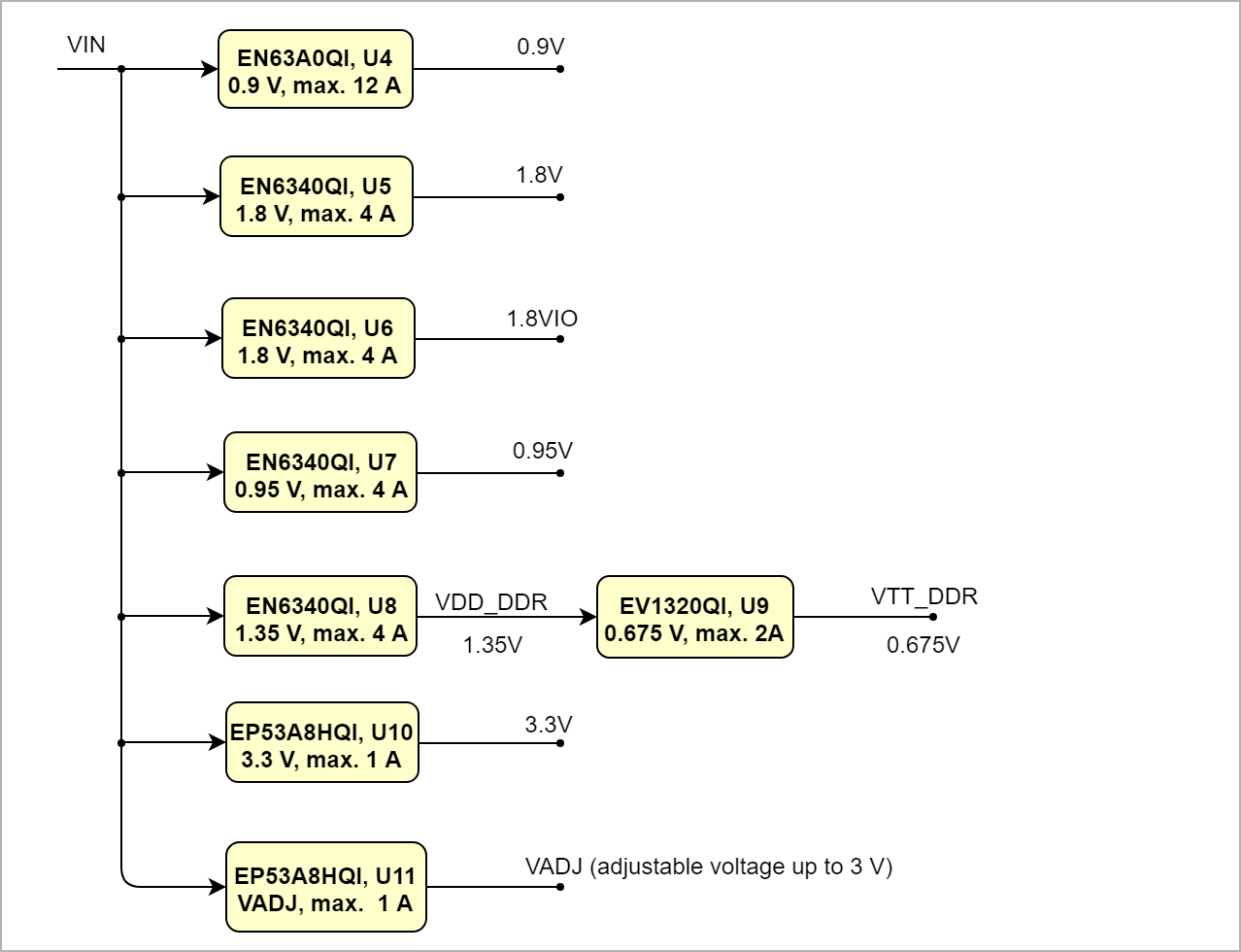
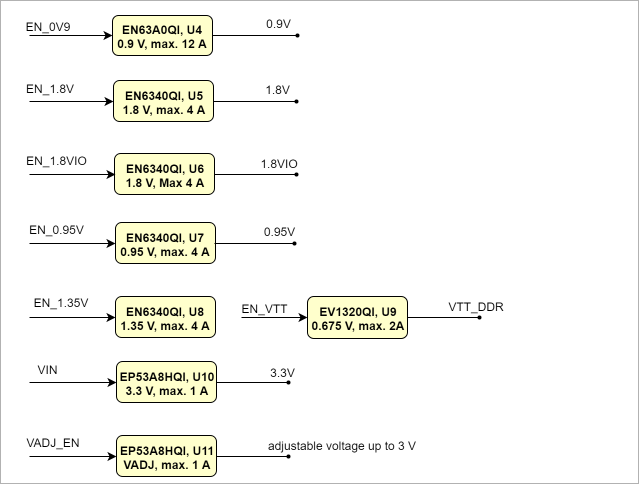
Power and Power-On Sequence
In 'Power and Power-on Sequence' section there are three important digrams which must be drawn: - Power on-sequence
- Power distribution
- Voltage monitoring circuit
|
Power Supply
Power supply with minimum current capability of 1 A for system startup is recommended.
Power Consumption
| FPGA | Typical Current |
|---|
| Intel Cyclone 10 GX | TBD* | | Intel MAX 10 | TBD* |
|
* TBD - To Be Determined
Power Distribution Dependencies
Power-On Sequence
Voltage regulators can be enabled through U18 (Intel MAX 10) - Bank 5 and 6.
Power Rails
| Power Rail Name | B2B Connector J1 Pin | B2B Connector J2 Pin | B2B Connector J3 Pin | Voltage Level | Direction | Notes |
|---|
| VIN | 145, 147,149, 151, 153, 155, 157, 159 | - | - | 5 V | Input |
| | VCCIO2K | 53, 54 | - | - | 1.2 V, 1.25 V, 1.35 V, 1.5 V or 1.8 V | Input |
| | VADJ | 140,142 | - | - | adjustable between 1.8 V - 3.0 V | Output | Voltages according to EP53A8HQI datasheet but restricted to allowed bank voltage | | VCCIO2J | - | 29,30 | - | 1.2 V, 1.25 V, 1.35 V, 1.5 V or 1.8 V | Input |
| 3.3V | - | 149,150 | - | 3.3 V | Output |
| | 1.8_VIO | - | - | 139 | 1.8 V | Output |
|
|
Bank Voltages
| FPGA | FPGA Bank | Voltage Level | Notes |
|---|
| Intel Cyclone 10 GX | Bank 1C | 0.95 V |
| Bank 1D | 0.95 V |
| | Bank 2A | 1.8 V | 1.8VIO | | Bank 2J | 1.2 V, 1.25 V, 1.35 V, 1.5 V or 1.8 V | VCCIO2J | | Bank 2K | 1.2 V, 1.25 V, 1.35 V, 1.5 V or 1.8 V | VCCIO2K | | Bank 2L | adjustable between 1.8 V - 3.0 V | Voltages according to EP53A8HQI datasheet | | Bank 3A | 1.35 V | VDD_DDR | | Bank 3B | 1.35 V | VDD_DDR | | Intel Max 10 | Bank 1A | 3.3 V |
| | Bank 1B | 3.3 V |
| | Bank 2 | 1.8 V | 1.8VIO | | Bank 3 | 1.8 V | 1.8VIO | | Bank 5 | 3.3V |
| | Bank 6 | 3.3V |
| | Bank 8 | 3.3V |
|
|
Board to Board Connectors
- This section is optional and only for modules.
use "include page" macro and link to the general B2B connector page of the module series, For example: 6 x 6 SoM LSHM B2B Connectors

|

Technical Specifications
Absolute Maximum Ratings
| Symbols | Description | Min | Max | Unit | Note |
|---|
| VIN | Power supply | -0.3 | 6.0 | V | Detemined by U10. | | VCCIO - 3 V I/O | I/O buffers power supply | -0.5 | 4.10 | V | Intel Cyclone 10 GX | | VCCIO - LVDS I/O | I/O buffers power supply | -0.5 | 2.46 | V | Intel Cyclone 10 GX | | VADJ | Adjustable voltage | -0.5 | 4.10 | V | Intel Cyclone 10 GX | | T_STG | Storage temperature | -40 | 85 | °C |
|
|
Recommended Operating Conditions
Operating temperature range depends also on customer design and cooling solution. Please contact us for options.
| Parameter | Min | Max | Unit | Reference Document |
|---|
| VIN | 5.0 | 5.0 | V |
| | VCCIO | 2.85 | 3.15 | V | See Intel Cyclone 10 GX datasheet. | | VADJ | 2.85 | 3.15 | V | VCCIO |
|
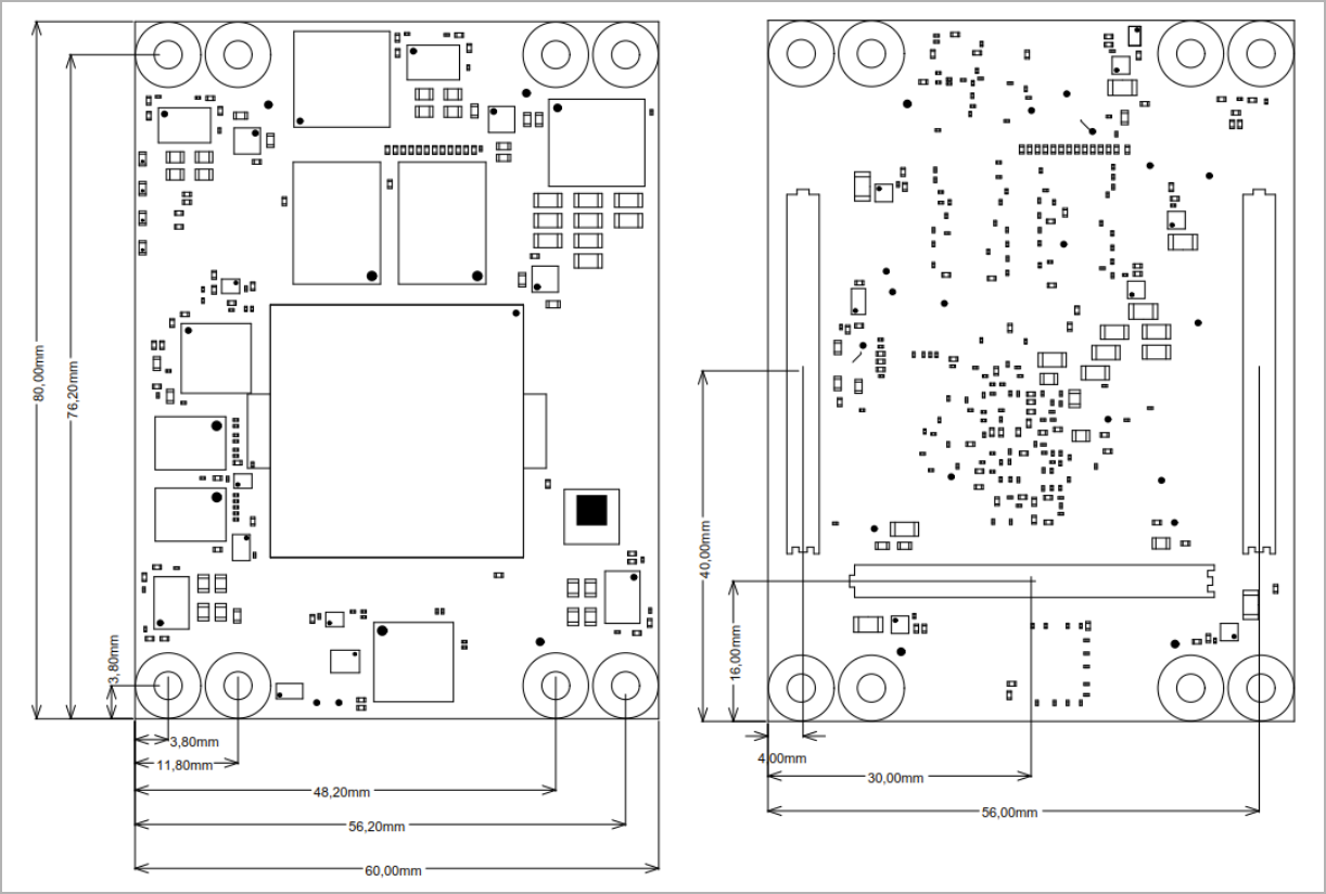
Physical Dimensions
Currently Offered Variants
Revision History
Hardware Revision History
| Date | Revision | Changes | Documentation Link |
|---|
| 202-12-23 | 03 | - two input cloock signals on B2B connected directly to GXBL1C bank
| REV03 | | 2019-09-11 | 02 | - added 100MHz MEMS oscillator, remove CLKUSR signal from J2
- replaced U21/U15 by SiT8008
- added pull-up to M10_NSTATUS signal
- added pull-up to M10_DEVCLRN, removed signal from J2
- added optional CryptoAuthentication chip U19
| REV02 | | 2018-08-10 | 01 | - | REV01 |
|
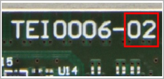
Hardware revision number can be found on the PCB board together with the module model number separated by the dash.
Document Change History
- Note this list must be only updated, if the document is online on public doc!
- It's semi automatically, so do following
Add new row below first Copy "Page Information Macro(date)" Macro-Preview, Metadata Version number, Author Name and description to the empty row. Important Revision number must be the same as the Wiki document revision number Update Metadata = "Page Information Macro (current-version)" Preview+1 and add Author and change description. --> this point is will be deleted on newer pdf export template - Metadata is only used of compatibility of older exports
|
| Date | Revision | Contributor | Description |
|---|
| | 
| - corrected Bank Voltages for Bank 2J (VCCIO2J) and Bank 2K (VCCIO2K)
| | 2022-03-18 | v.85 | Vitali Tsiukala | - Added Info about Gigabit Transceivers
| | 2021-06-07 | | Martin Rohrmüller | - corrected Physical Dimension figure
- updated to REV03
| | v.82 | Martin Rohrmüller | | 2019-06-14 | v.80 | Pedram Babakhani | Figures updated - Technical specifications updated
| | v.69 | Pedram Babakhani | | -- | all | 
| |
|
Disclaimer