Template Revision 2.3
TRM Name always "TE Series Name" +TRM, for example "TE0720 TRM" |
<!-- tables have all same width (web max 1200px and pdf full page(640px), flexible width or fix width on menu for single column can be used as before) -->
<style>
.wrapped{
  width: 100% !important;
  max-width: 1200px !important;
 }
</style> |
----------------------------------------------------------------------- |
Note for Download Link of the Scroll ignore macro: |
Table of Contents 
|
Overview
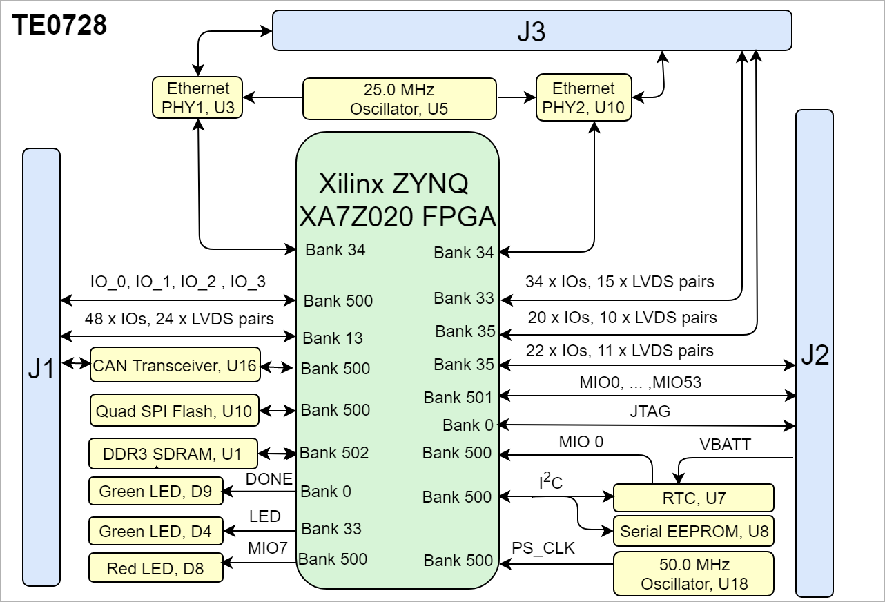
Trenz Electronic TE0728 is an automotive-grade FPGA module integrating an Automotive Xilinx Zynq-7 FPGA, two 100 Mbit Ethernet transceivers (PHY) , 512 MByte DDR3L SDRAM, 16 MByte Flash memory for configuration and operation, and powerful switching-mode power supplies for all on-board voltages. Numerous configurable I/Os are provided via rugged high-speed strips.
Within the complete module only Automotive components are installed.
All this in a compact 6 x 6 cm form factor, at the most competitive price.
Refer to http://trenz.org/te0728-info for the current online version of this manual and other available documentation.
Key Features
- Xilinx XA7Z020-1CLG484Q (Automotive)
- Rugged for shock and high vibration
- Dimensions: 6 x 6 cm
- Temperature range: Automotive
- Dual-Core ARM Cortex-A9 MPCore
- 2 x 100 MBit Ethernet transceiver (PHY)
DDR3L SDRAM, 16-bit-width - QSPI Flash memory (with XiP support)
- Plug-on module with 3 x 80-pin Samtec Micro Tiger Eye(TM) high-speed connectors
- 76 single ended I/O, 24 LVDS pairs (48 I/O) and 42 MIO available on board-to-board connectors
- CAN transceiver (PHY)
- 12 V power supply with watchdog
- On-board high-efficiency DC-DC converters
- System management and power sequencing
- eFUSE bit-stream encryption
- AES bit-stream encryption
- Temperature compensated RTC (real-time clock)
- Three user LEDs
- Evenly-spread supply pins for good signal integrity
Depending on the customer design, additional cooling might be required.
Block Diagram
Main Components
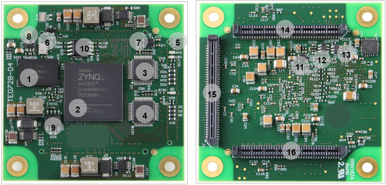
Notes : - Picture of the PCB (top and bottom side) with labels of important components
- Add List below
|
- DDR3 SDRAM, U1
- Xilinx Automotive XA7Z020-1CLG484Q ,U2
- 100 MBit Ethernet transceiver, U3
- 100 MBit Ethernet transceiver, U10
- User LED Green, D4
- Real Time Clock, Micro Crystal @32.768 MHz, U7
- Standard Clock Oscillators @ 25MHz, U5
- 64 Kbit I2C EEPROM, U11
- CAN Tranceiver, U16
- QSPI Nor Flash memory, U13
- Standard Clock Oscillators @ 50MHz, U14
- Low-Quiescent-Current Programmable Delay Supervisory Circuit, U15
- Low-Quiescent-Current Proggrammable Delay Supervisory Circuit, U12
- B2B connector , JM2
- B2B connector , JM3
- B2B connector Samtec Micro Tiger Eye Connector SEM-140-02-03, JM1
Initial Delivery State

Storage Device | Symbol | Content |
|---|
Quad SPI Flash | U13 | Not Programmed | | EEPROM | U11 | Not Programmed |
|
Control Signals
- Overview of Boot Mode, Reset, Enables,
|
Boot Mode

Signal | FPGA Bank | Pin | B2B | Signal State | Boot Mode |
|---|
Boot_R | 500 | E4 | J2-11 | Low | QSPI | | High | SD Card |
|
Reset
Zynq-7020SoC includes a reset that is driven by the reset system. Hardware resets are driven by the power-on reset signal (Reset) connected to carrier and the system reset signal (PS_SRST_B) connected to VMIO, it means after power on the PS will be reset.

Signal | B2B | I/O | Note |
|---|
Reset | J2-7 | Input | Comes from Carrier | | RST_OUT | J2-9 | Output | PS_PROB_B |
|
Signals, Interfaces and Pins
Notes : - For carrier or stand-alone boards use subsection for every connector type (add designator on description, not on the subsection title), for example:
- For modules which needs carrier use only classes and refer to B2B connector if more than one is used, for example
|
Board to Board (B2B) I/Os
FPGA bank number and number of I/O signals connected to the B2B connector:

| FPGA Bank | Type | B2B Connector | I/O Signal Count | Voltage Level | Notes |
|---|
| 13 | HR | J1 | 48(24) | VCCO_13 | variable from carrier | | 500 | HR | J1 | 4 | 3.3V |
| | 501 | HR | J2 | 37 | VMIO1 | variable from carrier | | 33 | HR | J3 | 34 | 3.3V |
| | 35 | HR | J3 | 20 | 3.3V |
| | 35 | HR | J2 | 22 | 3.3V |
|
|
Ethernet PHY
Ethernet pins connections to Board to Board (B2B). Ethernet components ETH1 and ETH2 are connected to B2B connector J3.

| Schematic | ETH1 | ETH2 | Direction | Pullup | Notes |
|---|
| CTREF | J3-57 | J3-25 | In |
| Magnetics center tap voltage | | TD+ | J3-58 | J3-28 | Out | on-board | Transfer | | TD- | J3-56 | J3-26 | Out | on-board |
| | RD+ | J3-52 | J3-22 | In | on-board | Recieve | | RD- | J3-50 | J3-20 | In | on-board |
| | LED1 | J3-55 | J3-23 | Out | on-board | LED Yellow on carrier | | LED2 | J3-53 | J3-21 | Out | on-board |
| | LED3 | J3-51 | J3-19 | Out | on-board | LED Green on carrier | | POWERDOWN/INT | L21 | R20 | In | on-chip |
| | RESET_N | M15 | R16 | In | on-chip | Active low PHY Reset |
|
CAN PHY
CAN pins connections to Board to Board (B2B).

| Schematic | B2B | MIO Pin | Direction | Notes |
|---|
| CANH/CANL | J1-2/J1-4 | - | Inout/Inout |
| | TX/RX |
| MIO8/MIO9 | Out/In |
|
|
JTAG Interface
JTAG access to the Xilinx XA7Z020 FPGA through B2B connector JM2.

JTAG Signal | B2B Pin |
|---|
| TMS | J2-12 | | TDI | J2-10 | | TDO | J2-8 | | TCK | J2-6 |
|
MIO Pins

| MIO Pin | Schematic | B2B | Direction | Pullup | Notes |
|---|
| MIO0 | MIO0 | - |
| Enable | RTC interrupt | | MIO1 | SPI_CS | - | Out | Enable | SPI Flash | | MIO2-5 | SPI_DQ0..SPI_DQ3/M0...M3 | - | Inout | Disable | SPI Flash | | MIO6 | SPI_SCK/M4 | - | Out | Disable | SPI Flash clock | | MIO7 | LED RED | - | Out | Disable | LED | | MIO8 | TX | - | Out | Disable | CAN Transceiver | | MIO9 | RX | - | Out | Enable | CAN Transceiver | | MIO10 | IO_0 | J1-7 | Inout | Enable | GPIO | | MIO11 | IO_1 | J1-9 | Inout | Enable | GPIO | | MIO12 | IO_2 | J1-11 | Inout | Enable | GPIO | | MIO13 | IO_3 | J1-13 | Inout | Enable | GPIO | | MIO14 | SCL | - | Inout | Enable | I2C | | MIO15 | SDA | - | Inout | Enable | I2C | | MIO16 | - | J2-17 | Inout | Enable | GPIO | | MIO17 | - | J2-18 | Inout | Enable | GPIO | | MIO18 | - | J2-27 | Inout | Enable | GPIO | | MIO19 | - | J2-23 | Inout | Enable | GPIO | | MIO20 | - | J2-28 | Inout | Enable | GPIO | | MIO21 | - | J2-22 | Inout | Enable | GPIO | | MIO22 | - | J2-26 | Inout | Enable | GPIO | | MIO23 | - | J2-20 | Inout | Enable | GPIO | | MIO24 | - | J2-24 | Inout | Enable | GPIO | | MIO25 | - | J2-21 | Inout | Enable | GPIO | | MIO26 | - | J2-25 | Inout | Enable | GPIO | | MIO27 | - | J2-19 | Inout | Enable | GPIO | | MIO28 | Tx_clk | J2-51 | Out | Enable | ETH | | MIO29 | Txd0 | J2-44 | Out | Enable | ETH | | MIO30 | Txd1 | J2-49 | Out | Enable | ETH | | MIO31 | Txd2 | J2-43 | Out | Enable | ETH | | MIO32 | Txd3 | J2-42 | Out | Enable | ETH | | MIO33 | Tx_ctl | J2-46 | Out | Enable | ETH | | MIO34 | Rx_clk | J2-48 | In | Enable | ETH | | MIO35 | Rxd0 | J2-47 | In | Enable | ETH | | MIO36 | Rxd1 | J2-41 | In | Enable | ETH | | MIO37 | Rxd2 | J2-52 | In | Enable | ETH | | MIO38 | Rxd3 | J2-45 | In | Enable | ETH | | MIO39 | Rx_ctl | J2-50 | In | Enable | ETH | | MIO40 | CLK | J2-34 | Inout | Disable | SD on carrier | | MIO41 | Cmd | J2-29 | Inout | Disable | SD on carrier | | MIO42 | Data0 | J2-37 | Inout | Disable | SD on carrier | | MIO43 | Data1 | J2-40 | Inout | Disable | SD on carrier | | MIO44 | Data2 | J2-32 | Inout | Disable | SD on carrier | | MIO45 | Data3 | J2-31 | Inout | Disable | SD on carrier | | MIO46 | wp | J2-35 | In | Enable | SD on carrier | | MIO47 | cd | J2-33 | In | Enable | SD on carrier | | MIO48 | MIO48 | J2-30 | Out | Enable | LED Red on Carrier | | MIO49 | MIO49 | J2-38 | Out | Enable | LED Yellow on Carrier | | MIO50 | MIO50 | J2-36 | Out | Enable | LED Green on Carrier | | MIO51 | MIO51 | J2-39 | Inout | Disable | GPIO | | MIO52 | UART_Txd | J2-15 | Out | Enable | UART transfer | | MIO53 | UART_Rxd | J2-16 | In | Enable | UART receive |
|
On-board Peripherals
Notes : - add subsection for every component which is important for design, for example:
- Two 100 Mbit Ethernet Transciever PHY
- USB PHY
- Programmable Clock Generator
- Oscillators
- eMMCs
- RTC
- FTDI
- ...
- DIP-Switches
- Buttons
- LEDs
|

| Chip/Interface | Product | Notes |
|---|
| SPI Flash | U13 | 16 MByte Flash | | EEPROM | U11 | 64 Kbit EEPROM | | RTC | U7 | Real Time Clock | | DDR3 SDRAM | U1 | Volatile Memory | | Ethernet | U3, U10 | Two 100 Mbit Ethernet | | CAN Transceiver | U16 |
| | User LED | D4 | Green LED |
|
Quad SPI Flash Memory
On-board QSPI flash memory is used to store initial FPGA configuration. Datasheet is provided in Texas Instruments. Besides FPGA configuration, remaining free flash memory can be used for user application and data storage. All four SPI data lines are connected to the FPGA allowing x1, x2 or x4 data bus widths. Maximum data rate depends on the selected bus width and clock frequency.
Quad SPI Flash (U7) is connected to the Zynq PS QSPI0 interface via PS MIO bank 500.

| MIO Pin | Schematic | Pin | Notes |
|---|
| MIO1 | SPI_CS | U13-A1 |
| | MIO2 | SPI_DQ0/M0 | U13-A2 |
| | MIO3 | SPI_DQ1/M1 | U13-F6 |
| | MIO4 | SPI_DQ2/M2 | U13-E4 |
| | MIO5 | SPI_DQ3/M3 | U13-A3 |
| | MIO6 | SPI_SCK/M4 | U13-A4 |
|
|
RTC
The RTC has an I2C Bus (2-wire SerialInterface) and offers temperature compensated time. The STC-Smart Temperature Compensation is calibrated in the factory and leads to a very high time-accuracy.
RTC intruppt is connected to MIO0 connected to Bank 500 through pin G6.

| MIO Pin | Schematic | Pin | Notes |
|---|
| MIO15 | SDA | U7-5 | On-board RTC, and EEPROM | | MIO14 | SCL | U7-4 | On-board RTC, and EEPROM |
|

| I2C Device | I2C Address | IC | Notes |
|---|
| RTC | 0x68 | U7 |
| | EEPROM | 0XA0 | U11 |
|
|
EEPROM
The Microchip Technology Inc. 24xx64 is a 64 Kbit Electrically Erasable PROM. The device is organized as a single block of 8K x 8-bit memory with a 2-wire serial interface. The 24xx64 also has a page write capability for up to 32 bytes of data. Functional address lines allow up to eight devices on the same bus, for up to 512 Kbits address space.

| MIO Pin | Schematic | Pin | Notes |
|---|
| MIO15 | SDA | U11-3 | On-board RTC, and EEPROM | | MIO14 | SCL | U11-1 | On-board RTC, and EEPROM |
|
LEDs

| Schematic | Color | Connected to | Active Level | IO Standard |
|---|
| D9 | Green | DONE | Low | not applicable | | D8 | RED | MIO7 | High | not applicable | | D4 | Green | Bank 33 - V18 | High | LVCMOS33 |
|
DDR3 SDRAM
The TE0728 SoM has a volatile DDR3 SDRAM IC for storing user application code and data. Size of DDR3 can be varied in different assembly versions.
Configuration of the DDR3 memory controller in the FPGA should be done using the MIG tool in the Xilinx Vivado Design Suite IP catalog.
Ethernet
There are two 100 MBit Extreme Temperature Ethernet provided by Texas Instrument on the board. Datasheet is provided at TI website. Both PHY's are connected with all I/O Pins to FPGA Bank 34 (VCCIO = 3.3V). PHY Clock 25 MHz source is provided from MEMS Oscillator. There is no sharing of signals for the two PHY's.
PUDC pin is connected with pull-up to 3.3V those pre-configuration pull-ups are disabled by default. Strapping resistor exist to change the PUDC mode.

| Schematic | ETH1 | ETH2 | Pullup | Notes |
|---|
| CTREF | J3-57 | J3-25 |
| Magnetics center tap voltage | | TD+ | J3-58 | J3-28 | on-board |
| | TD- | J3-56 | J3-26 | on-board |
| | RD+ | J3-52 | J3-22 | on-board |
| | RD- | J3-50 | J3-20 | on-board |
| | LED1 | J3-55 | J3-23 | on-board | LED Yellow on Carrier - ACK | | LED2 | J3-53 | J3-21 | on-board | Speed | | LED3 | J3-51 | J3-19 | on-board | LED Green on Carrier- Link | | POWERDOWN/INT | L21 | R20 | on-chip |
| | RESET_N | M15 | R16 | on-chip |
|
|
CAN Transceiver
Controller Area Network (CAN) transceivers are designed for use with the Texas Instruments TMS320Lx240x 3.3-V DSPs with CAN controllers. The datasheet is available in TI website. Each CAN transceiver is designed to provide differential transmit capability to the bus and differential receive capability to a CAN controller at speeds up to 1 Mbps.

| MIO Pin | Schematic | Pin | Notes |
|---|
| MIO8 | D - Tx | U16-1 | Driver Input | | MIO9 | R - Rx | U16-4 | Reciever Output |
|
Clock Sources

| IC | Description | Frequency | Used as |
|---|
| U14 | MEMS Oscillator | 50 MHz | PS PLL clock | | U5 | MEMS Oscillator | 25 MHz | Ethernet PHY Clock | | U7 | RTC (internal oscillator) | 32.768 KHz | Used by RTC, CLKOUT of RTC not connected |
|
Power and Power-On Sequence
Power Supply
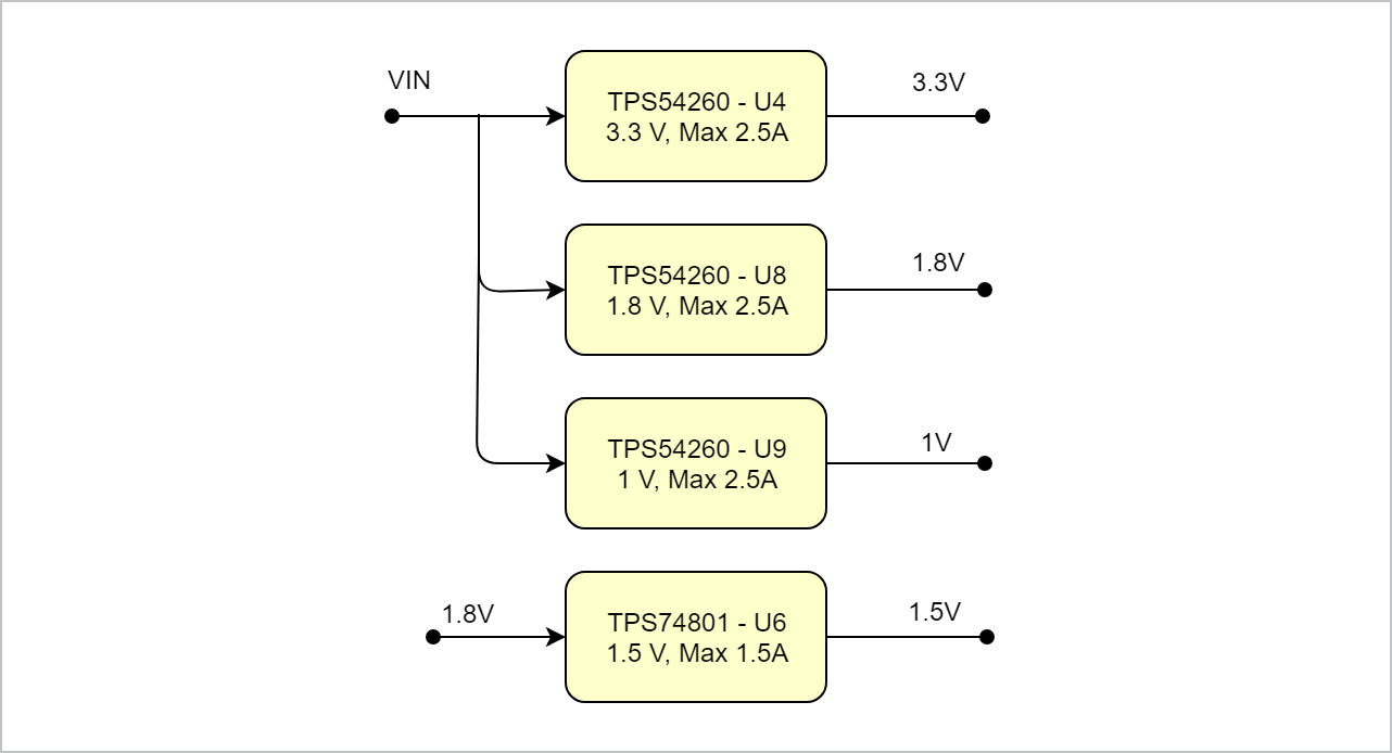
Power supply with minimum current capability of 2.5A for system startup is recommended.
Power Consumption

| Power Input Pin | Typical Current |
|---|
| VIN | TBD* |
|
* TBD - To Be Determined
Power on Sequence
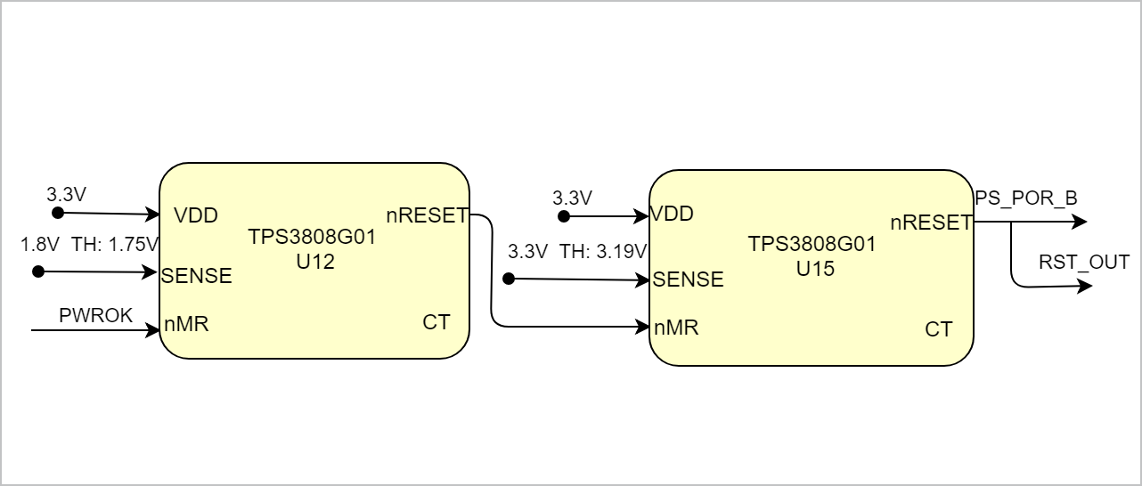
The TE07028 SoM meets the recommended criteria to power up the Xilinx Zynq properly by keeping a specific sequence of enabling the on-board DC-DC converters and regulators dedicated to the particular functional units of the Zynq chip and powering up the on-board voltages. When the U8 and U9 generates PWRGD signal, it turns on the U4 which generates PWRGD_3.3V, it turns on the U6 and it generates PWROK signal which is connected to MR. Whenever the supply voltage for U12 drops down below the threshold it resets the system. Actually it resets the system when all regulators are working.
Power Distribution Dependencies
Voltage Monitor Circuit
The microprocessor supervisory circuits monitor system voltages asserting an open-drain RESET signal when the SENSE voltage drops below a preset threshold or when the manual reset (MR) pin drops to a logic low. The RESET output remains low for the user adjustable delay time after the SENSE voltage and MR return above their thresholds. Datasheet is available in Texas Instruments website.
Power Rails

B2B Name | B2B JM1 Pin | B2B JM2 Pin | B2B JM3 Pin | Direction | Notes |
|---|
| VIN | 1,3 | - | - | Input | Supply voltage from carrier board. | | VCCO_13 | 39 | - | - | I/O |
| | VBATT | - | 1 | - | Output | RTC Supply voltage | | 3.3V | 19 | 4 | 25,57 | Output | Internal 3.3V voltage level. | | VMIO | - | 2 |
| Input | 3.3V from carrier | 1.8V | - | 5 | - | Output | Internal 1.8V voltage level. |
|
Bank Voltages

| Schematic Name | | HP I/O Bank | Notes |
|---|
| 500 | VCCO_MIO0_500 | 3.3V | Supported |
| | 501 | VCCO_MIO1_501 | 2.5V or 3.3V | Supported | supplied by 3.3V from carrier. | | 502 | VCCO_DDR_502 | 1.5V | Supported |
| | 13 | VCCO_13 | 1.8V or 3.3V | Supported | Supplied by the carrier board. J1 | | 33 | 3.3V | 3.3V | Supported | Supplied by carrier board. J3 | | 34 | 3.3V | 3.3V | Supported |
| | 35 | 3.3V | 3.3V | Supported | Supplied by the carrier board. J2, J3 |
|
Board to Board Connectors

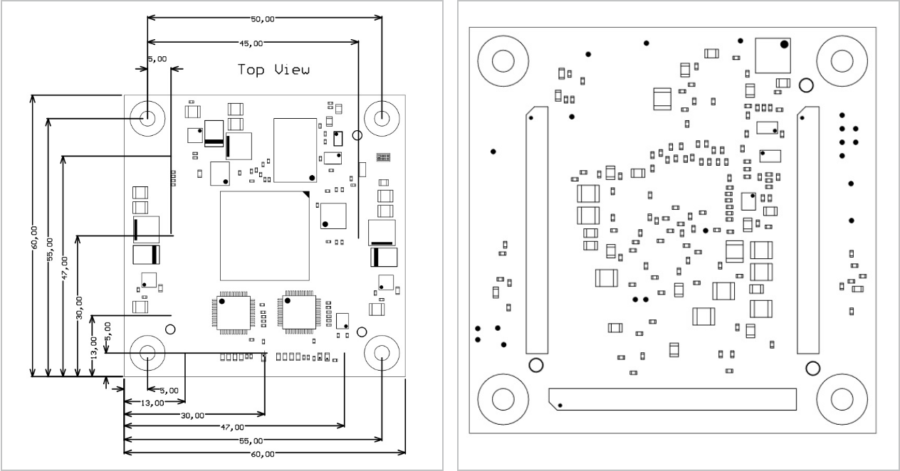
6 x 6 modules use two or three Samtec Micro Tiger Eye Connector on the bottom side.
Technical Specifications
Absolute Maximum Ratings
Processing System(PS)

| Symbols | Description | Min | Max | Unit |
|---|
| VCCPINT | PS internal logic supply voltage | -0.5 | 1.1 | V | | VCCPAUX | PS auxiliary supply voltage | -0.5 | 2.0 | V | | VCCPLL | PS PLL supply | -0.5 | 2.0 | V | | VCCO_DDR | PS DDR I/O supply voltage | -0.5 | 2.0 | V | | VPREF | PS input reference voltage | -0.5 | 2.0 | V | | VCCO_MIO0 | PS MIO I/O supply voltage for HR I/O banks | -0.5 | 3.6 | V | | VCCO_MIO1 | PS MIO I/O supply voltage for HR I/O banks | 1.71 | 3.45 | V | | VCCINT | PL internal logic supply voltage | -0.5 | 1.1 | V | | VCCPAUX | PL auxiliary supply voltage | -0.5 | 2.0 | V | | VCCPLL | PL PLL supply | -0.5 | 1.1 | V | | VPREF | PL input reference voltage | -0.5 | 2.0 | V | | VCCO | PL supply voltage for HR I/O banks | -0.5 | 3.6 | V | | VIN | I/O input voltage for HR I/O banks | 1.71 | 3.45 | V |
|
Recommended Operating Conditionse

| Parameter | Min | Max | Units | Reference Document |
|---|
| VIN supply voltage | 3.5 | 60 | V | TPS54260-Q1 datasheets. | | Supply voltage for PS MIO banks | 1.71 | 3.465 | V | See Xilinx DS187 datasheet. | | I/O input voltage for PS MIO banks | -0.2 | VCCO_MIO + 0.20 | V | See Xilinx DS187 datasheet. | | Supply voltage for PS DDR | 1.14 | 1.89 | V | See Xilinx DS187 datasheet. | | I/O input voltage for PS DDR | -0.20 | VCCO_DDR + 0.20 | V | See Xilinx DS187 datasheet. | | Supply voltage for HR I/Os banks | 1.14 | 3.465 | V | See Xilinx DS187 datasheet. | | I/O input voltage for HR I/O banks | -0.20 | VCCIO + 0.20 | V | See Xilinx DS187 datasheet. | | Storage Temperature | -40 | +125 | °C |
| | Operating Temperature | -40 | +105 | °C |
|
|
Physical Dimensions
Variants Currently In Production
Revision History
Hardware Revision History
Hardware revision number is printed on the PCB board next to the module model number separated by the dash.
Document Change History
- Note this list must be only updated, if the document is online on public doc!
- It's semi automatically, so do following
Add new row below first Copy "Page Information Macro(date)" Macro-Preview, Metadata Version number, Author Name and description to the empty row. Important Revision number must be the same as the Wiki document revision number Update Metadata = "Page Information Macro (current-version)" Preview+1 and add Author and change description. --> this point is will be deleted on newer pdf export template - Metadata is only used of compatibility of older exports
|

| Date | Revision | Contributor | Description |
|---|
| 

| 
| | -- | all | 
| |
|
Disclaimer


