Template Revision 2.6
- Module: TRM Name always "TE Series Name" +TRM
Example: "TE0728 TRM" - Carrier: TRM Name usually "TEB Series Name" +TRM
Example: "TEB0728 TRM"
|
<!-- tables have all same width (web max 1200px and pdf full page(640px), flexible width or fix width on menu for single column can be used as before) -->
<style>
.wrapped{
  width: 100% !important;
  max-width: 1200px !important;
 }
</style> |
----------------------------------------------------------------------- |
Note for Download Link of the Scroll ignore macro: |
Table of Contents 
|
Overview
The Trenz Electronic TEI0016 is a commercial-grade module based on Intel® MAX 10. Intel MAX 10 devices are the ideal solution for system management, I/O expansion, communication control planes, industrial, automotive, and consumer applications.
Refer to http://trenz.org/tei0016-info for the current online version of this manual and other available documentation.
Key Features
Intel® MAX 10 Commercial [10M08SAU169C8G]
SDRAM Memory up to 32 Mbyte (8Mbyte default)
USB 2.0 Multipurpose UART/FIFO IC (FT2232H)
- 4 Kbit EEPROM Memory for FTDI configuration data
- Micro USB Receptacle (communication and power)
SPI Flash - NOT INSTALLED (only special option)
- 8x User LED
Micro USB Connector
16 Bit Analog to Digital Converter with 1 MSPS or 500 kSPS
2x SMA Female Connector
I/O interface: 23x GPIO
Power Supply: 5V (from USB)
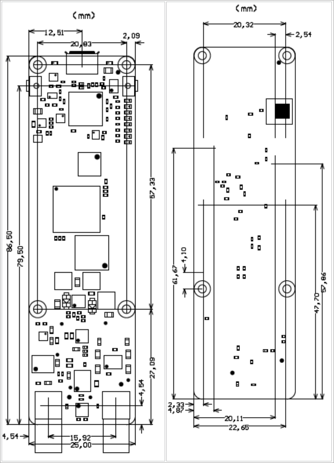
Dimension: 25 mm x 86.5 mm
Others:
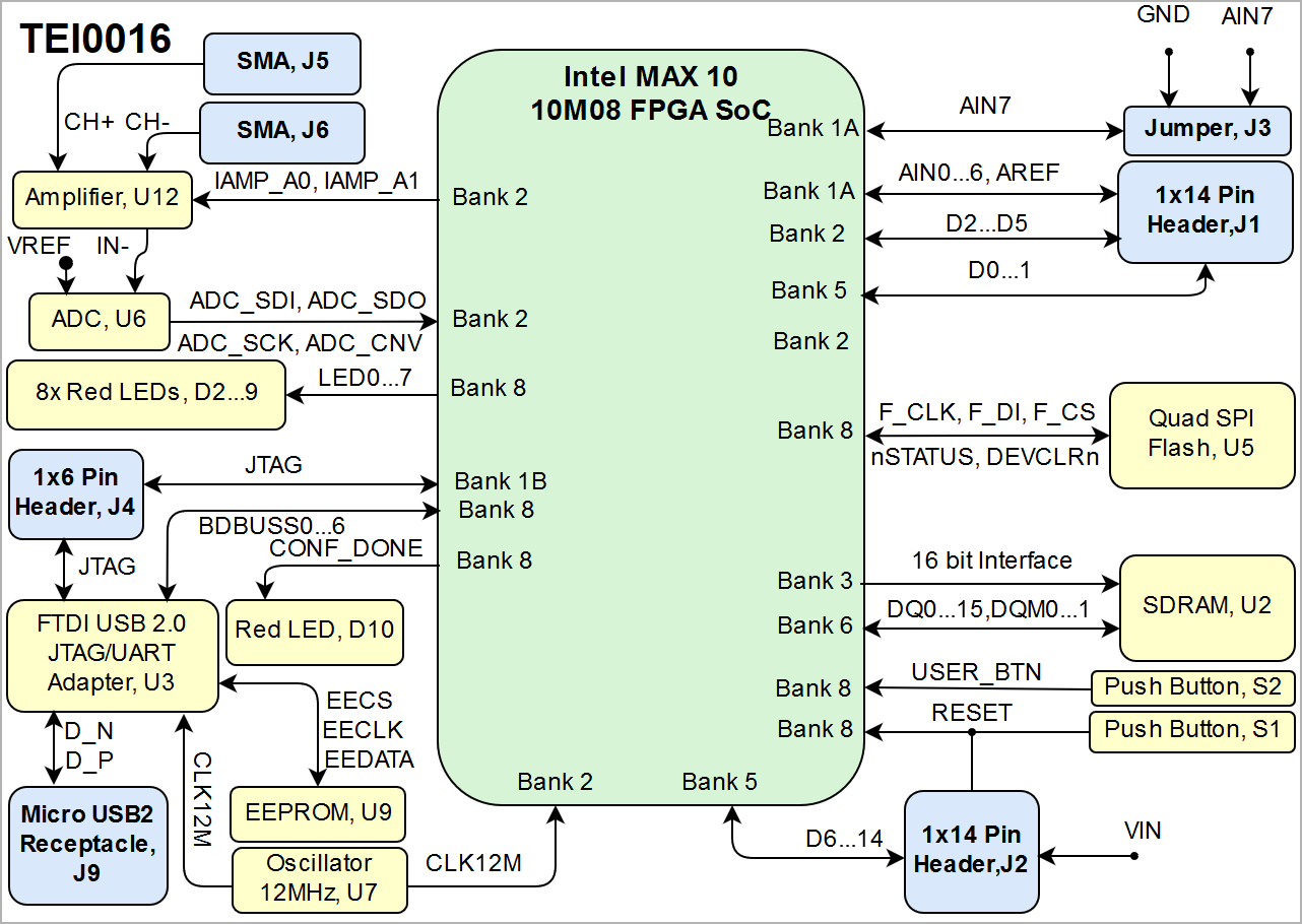
Block Diagram
Main Components
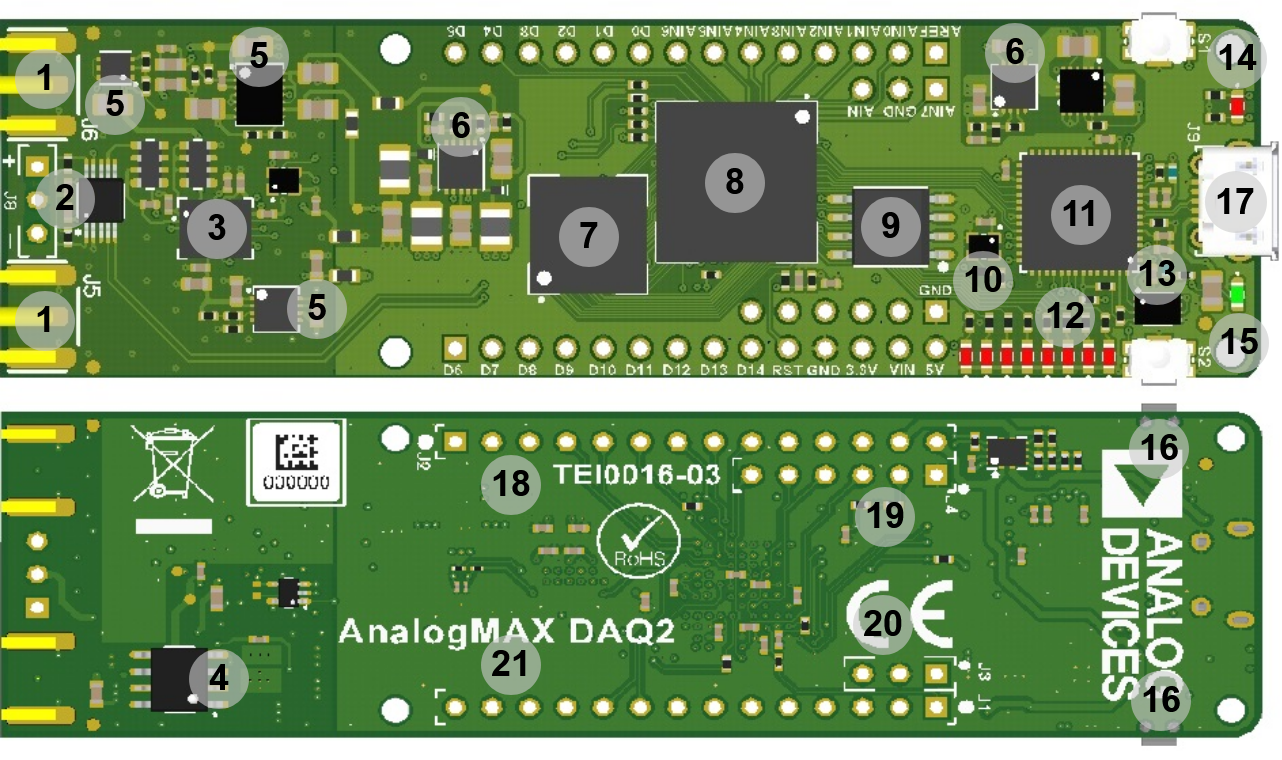
Notes : - Picture of the PCB (top and bottom side) with labels of important components
- Add List below
|
- SMA Connector, J5...6
- Amplifier, U12
- Analog to Digital Converter, U6
- Voltage Reference, U8
- Voltage Regulator, U10 - U13 - U16
- Switching Voltage Regulator/LDO, U11 - U4
- SDRAM Memory, U2
- Intel® MAX 10 FPGA, U1
- SPI Flash Memory, U5 (not populated)
- 12.00 MHz MEMS oscillator, U7
- FTDI USB to JTAG/UART/FIFO, U3
- User LEDs, D2...9
- 4Kb EEPROM, U9
- Configuration LED (Red) , D10
- Power-on LED (Green), D1
- Push button, S1...2
- Micro USB Connector, J9
- 1x14 pin header, J2 (Not assembled)
- 1x6 pin header, J4 (Not assembled)
- Jumper, J3
- 1x14 pin header, J1 (Not assembled)
Initial Delivery State
Notes : Only components like EEPROM, QSPI flash and DDR3 can be initialized by default at manufacture. If there is no components which might have initial data ( possible on carrier) you must keep the table empty |

Storage device name | Content | Notes |
|---|
Quad SPI Flash | N/A | Not populated | | EEPROM | Programmed | FTDI configuration |
|
Configuration Signals
- Overview of Boot Mode, Reset, Enables.
|
The FPGA configuration for Intel MAX 10 FPGAs can be stored through JTAG interface (using a *.POF file) on the FPGA itself since the Intel MAX 10 FPGA offers non-volatile configuration memory on chip. The FPGA configuration is loaded from the non-volatile memory when the board is powered up. To configure the FPGA directly, the JTAG interface can be used to configure the FPGA volatile (using a *.SOF file), means the configuration is lost after power off.
FPGA Reconfigration can be triggered by pressing push button S1.
Signal | Push Button | Pin Header | Note |
|---|
RESET | S1 | J2 | Connected to nCONFIG |
|
Signals, Interfaces and Pins
Notes : - For carrier or stand-alone boards use subsection for every connector type (add designator on description, not on the subsection title), for example:
- For modules which needs carrier use only classes and refer to B2B connector if more than one is used, for example
|
I/Os on Pin Headers and Connectors
| FPGA Bank | Connector Designator | I/O Signal Count | Voltage Level | Notes |
|---|
| Bank 1A | J1 | 7 | 3.3V | AIN0...6 | | Bank 1B | J4 | 5 | 3.3V | JTAG interface | | Bank 2 | J1 | 4 | 3.3V | DIO2...5 | | Bank 5 | J2 | 9 | 3.3V | DIO6...14 | | J1 | 2 | 3.3V | DIO0...1 | | Bank 8 | J2 | 1 | 3.3V | RESET |
|
FPGA I/O Banks
you must fill the table below with group of MIOs which are connected to a specific components or peripherals, you do not have to specify pins in B2B, Just mention which B2B is connected to MIOs. The rest is clear in the Schematic. Example: | MIO Pin | Connected to | B2B | Notes |
|---|
| MIO12...14 | SPI_CS , SPI_DQ0... SPI_DQ3 SPI_SCK | J2 | QSPI |
|
| FPGA Bank | I/O Signal Count | Connected to | Notes |
|---|
| Bank 1A | 7 | 1x14 Pin header, J1 | AIN0...6 | | 1 | Jumper, J3 | AIN7 | | Bank 1B | 5 | 1x6 Pin header, J4 | JTAG_EN, TDI, TDO, TMS, TCK | Bank 2
| 4 | 1x14 Pin header, J1 | D2...5 | | 5 | ADC, U15 | ADC_EN, ADC_SDI, ADC_SDO, ADC_SCK, ADC_CNV | | 1 | 12MHz Oscillator, U7 | CLK12M | | 2 | Amplifier, U12 | nIAMP_A0, nIAMP_A1 | | Bank 3 | 22 | SDRAM, U2 | RAM_ADDR_CMD | | Bank 5 | 9 | 1x14 Pin header, J2 | DIO6...14 | | 2 | 1x14 Pin header, J1 | DIO0...1 | | 1 | D12_R | DIO12 | | Bank 6 | 16 | SDRAM, U2 | DQ0...15 | | 2 | SDRAM, U2 | DQM0...1 | | 1 | D11_R | DIO11 | Bank 8
| 8 | User Red LEDs, D2...9 | LED0...7 | | 6 | SPI Flash, U5 | F_CS, F_CLK, F_DI, F_DO, nSTATUS, DEVCLRn | | 1 | Red LED, D10 | CONF_DONE | | 6 | FTDI JTAG/UART Adapter, U3 | BDBUS0...5 | | 1 | Push Button, S2 | USER_BTN |
|
Micro-USB Connector
The Micro-USB2 connector J9 provides an interface to access the UART and JTAG functions via FTDI FT2232 chip. The use of this feature requires that USB driver is installed on your host PC.
| Pins | Connected to | Note |
|---|
| VBUS | USB_VBUS |
| | D+ | FTDI U3, DP pin |
| | D- | FTDI U3, DM pin |
|
|
JTAG Interface
JTAG access to the TEI0016 SoM through pin header connector J4.
JTAG Signal | Pin Header Connector | Note |
|---|
| TMS | J4-6 |
| | TDI | J4-5 |
| | TDO | J4-4 |
| | TCK | J4-3 |
| | JTAG_EN | J4-2 | Pulled-up to 3.3V. |
|
On-board Peripherals
Notes : - add subsection for every component which is important for design, for example:
- Two 100 Mbit Ethernet Transciever PHY
- USB PHY
- Programmable Clock Generator
- Oscillators
- eMMCs
- RTC
- FTDI
- ...
- DIP-Switches
- Buttons
- LEDs
|
Notes : In the on-board peripheral table "chip/Interface" must be linked to the corresponding chapter or subsection |
SDRAM
TEI0016 is equipped with a Winbond 64 MBit (8 MByte) SDRAM chip in standard configuration, variants with 256 Mbit (32 MByte) memory density are also available. The SDRAM chip is connected to the FPGA bank 3 and 6 via 16-bit memory interface.
Notes : Minimum and Maximum density of quad SPI flash must be mentioned for other assembly options. |
| SDRAM I/O Signals | Signal Schematic Name | Connected to | Notes |
|---|
| Address inputs | A0 ... A13 | bank 3 | - | Bank address inputs
| BA0 / BA1 | bank 3 | - | | Data input/output | DQ0 ... DQ15 | bank 6 | - | | Data mask | DQM0 ... DQM1 | bank 6 | - | | Clock | CLK | bank 3 | - | | Control Signals | CS | bank 3 | Chip select | CKE | bank 3 | Clock enable | RAS | bank 3 | Row Address Strobe | CAS | bank 3 | Column Address Strobe | | WE | bank 3 | Write Enable |
|
FTDI FT2232H
The FTDI chip U3 converts signals from USB to a variety of standard serial and parallel interfaces. Refer to the FTDI data sheet to get information about the features of the FT2232H chip. FTDI FT2232H chip channel A is used in MPPSE mode for JTAG. Channel B is configured to be used as in async FIFO mode, this is default mode when using preprogrammed FTDI configuration. In this mode the communication from host PC looks like normal UART but from the FTDI side it is 8 bit FIFO style interface.
The configuration of FTDI FT2232H chip is pre-programmed on the EEPROM U9.
| FTDI Chip U3 Pin | Signal Schematic Name | Connected to | Notes |
|---|
| ADBUS0 | TCK | FPGA bank 1B, pin G2 | JTAG interface | | ADBUS1 | TDI | FPGA bank 1B, pin F5 | | ADBUS2 | TDO | FPGA bank 1B, pin F6 | | ADBUS3 | TMS | FPGA bank 1B, pin G1 | | BDBUS0 | BDBUS0 | FPGA bank 8, pin A4 | User configurable | | BDBUS1 | BDBUS1 | FPGA bank 8, pin B4 | User configurable | | BDBUS2 | BDBUS2 | FPGA bank 8, pin B5 | User configurable | | BDBUS3 | BDBUS3 | FPGA bank 8, pin A6 | User configurable | | BDBUS4 | BDBUS4 | FPGA bank 8, pin B6 | User configurable | | BDBUS5 | BDBUS5 | FPGA bank 8, pin A7 | User configurable | | BDBUS6 | BDBUS6 | FPGA bank 6, pin C11 |
| | BDBUS7 | BDBUS7 | FPGA bank 3, pin J7 |
| | BCBUS0 | BCBUS0 | FPGA bank 5, pin J9 |
| | BCBUS1 | BCBUS1 | FPGA bank 3, pin K5 |
| | BCBUS2 | BCBUS2 | FPGA bank 3, pin K5 |
| | BCBUS3 | BCBUS3 | FPGA bank 3, pin K5 |
| | BCBUS4 | BCBUS4 | FPGA bank 3, pin K5 |
|
|
SPI Flash
Optional SPI flash device maybe assembled in custom variants, normally it is not populated.
| Signal Schematic Name | Connected to | Notes |
|---|
| F_CS | FPGA bank 8, pin B3 | Chip select | | F_CLK | FPGA bank 8, pin A3 | Clock | | F_DI | FPGA bank 8, pin A2 | Data in / out | | nSTATUS | FPGA bank 8, pin C4 | Data in / out, configuration dual-purpose pin of FPGA | | DEVCLRN | FPGA bank 8, pin B9 | Data in / out, configuration dual-purpose pin of FPGA | | F_DO | FPGA bank 8, pin B2 | Data in / out |
|
EEPROM
The configuration of FTDI FT2232H chip is pre-programmed in the EEPROM U9.
| Schematic | Connected to | Notes |
|---|
EECS | FTDI U3, Pin EECS |
| | EECLK | FTDI U3, Pin EECLK |
| | EEDATA | FTDI U3, Pin EEDATA |
|
|
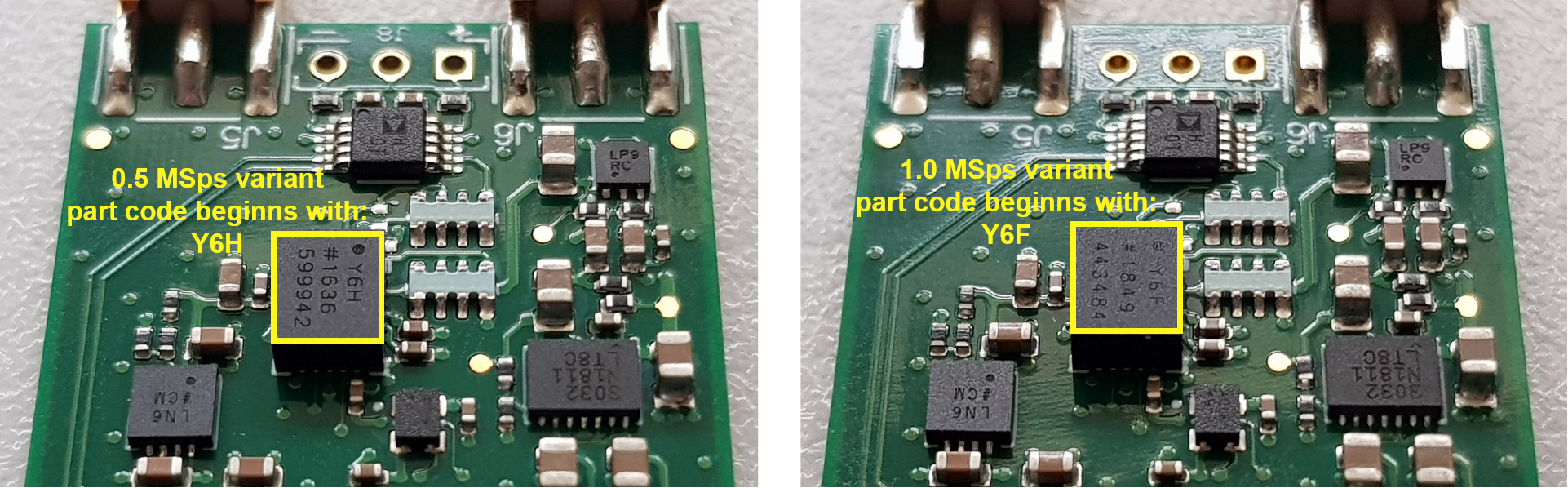
ADC
The boards with article nuber - TEI0016-03-08-C8A - are equipped with the Analog DevicesADC - ADAQ7988BCCZ - 16-bit 500kSPS,
boards wit article number TEI0016-03-08-C8B are equipped with the Analog Devices ADC - ADAQ7980BCCZ - 16-bit 1MSPS.
The ADC can be distinguished via its part code:
- TEI0016-03-08-C8A: ADAQ7988BCCZ - 16-bit 500kSPS - starts with Y6H
- TEI0016-03-08-C8B: ADAQ7980BCCZ - 16-bit 1.0MSPS - starts with Y6F
| Pins | Connected to | Notes |
|---|
IN+ | U8, VOUT |
| | IN- | U12, VOUT |
| | SDI | Bank 2, ADC_SDI |
| | SDO | Bank 2, ADC_SDO |
| | SCK | Bank 2, ADC_SCK |
| | CNV | Bank 2, ADC_CNV |
|
|
LEDs
| Designator | Color | Connected to | Active Level | Note |
|---|
| D2...9 | Red | LED1...8 | Active High | User LEDs | | D10 | Red | CONF_DONE | Active Low | Configuration DONE LED | | D1 | Green | 3.3V Power Rail | Active High | After power on it will be on. |
|
Push Buttons
| Designator | Connected to | Functionality | Note |
|---|
| S1 | RESET | General reset |
| | S2 | USER_BTN | User push button | Connected to FPGA Bank 8. |
|
Clock Sources
| Clock Source | Schematic Name | Frequency | Note |
|---|
| MEMS Oscillator, U7 | CLK12M | 12.00 MHz | Connected to FTDI FT2232 U3, pin 3. Connected to FPGA bank 2, pin H6. |
|
Power and Power-On Sequence
In 'Power and Power-on Sequence' section there are three important digrams which must be drawn: - Power on-sequence
- Power distribution
- Voltage monitoring circuit
|
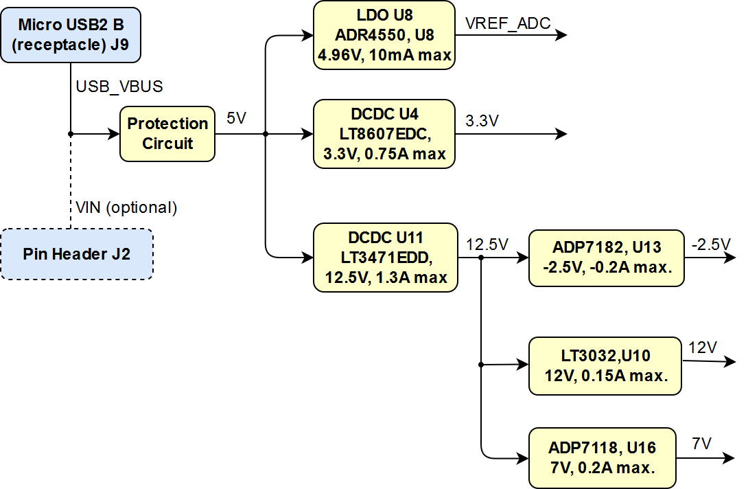
Power Supply
The module is supplied from USB (optionally via unpopulated pin header).
Power Consumption
| FPGA | Typical Current |
|---|
| Intel MAX 10 10M08 FPGA | TBD* |
|
* TBD - To Be Determined
Power Distribution Dependencies
Power-On Sequence
There is no specific or special power-on sequence, just one single power source is needed. After power on, the green LED (D1) will be on.
Power Rails
| Power Rail Name | Connector J2 Pin | Connector J9 Pin | Direction | Notes |
|---|
| VIN | J2-13 | - | Input | 5 V - Pin Header | | 3.3V | J2-12 | - | Output |
| | 5V | J2-14 | - | Output |
| USB_VBUS | - | J9-1 | Input | 5 V - USB Connector |
|
Bank Voltages
| Schematic Name | | Notes |
|---|
| Bank 1A | VCCIO1A | 3.3V |
| | Bank 1B | VCCIO1B | 3.3V |
| | Bank 2 | VCCIO2 | 3.3V |
| | Bank 3 | VCCIO3 | 3.3V |
| | Bank 5 | VCCIO5 | 3.3V |
| | Bank 6 | VCCIO6 | 3.3V |
| | Bank 8 | VCCIO8 | 3.3V |
|
|
Technical Specifications
Absolute Maximum Ratings
| Symbols | Description | Min | Max | Unit | Reference Document |
|---|
VIN | Supply voltage | 4.75 | 5.25 | V |
| | CH1-, CH1+ | Analog input voltage on amplifier U12 pin 1, 10 | -30 | 30 | V | AD8251 datasheet | T_STG | Storage Temperature | -40 | +85 | °C |
|
|
Recommended Operating Conditions
Operating temperature range depends also on customer design and cooling solution. Please contact us for options.
| Symbols | Min | Max | Unit | Reference Document |
|---|
| VIN supply voltage (5.0V nominal) | 4.75 | 5.25 | V |
| | Analog input voltage on amplifier U12 pin 1 (CH1-), 10 (CH1+) | -10 | 10 | V |
| | T_OP | 0 | +70 | °C | W9864G6JT-6 datasheet |
|
Physical Dimensions
Module size: 86.5 mm × 25 mm. Please download the assembly diagram for exact numbers.
PCB thickness: 1.22 mm.
Currently Offered Variants
Revision History
Hardware Revision History
| Date | Revision | Changes | Documentation Link |
|---|
| 2019-02-11 | 01 | - | REV01 |
|
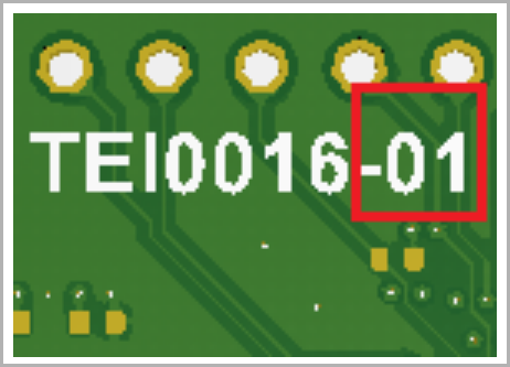
Hardware revision number can be found on the PCB board together with the module model number separated by the dash.
Document Change History
- Note this list must be only updated, if the document is online on public doc!
- It's semi automatically, so do following
Add new row below first Copy "Page Information Macro(date)" Macro-Preview, Metadata Version number, Author Name and description to the empty row. Important Revision number must be the same as the Wiki document revision number Update Metadata = "Page Information Macro (current-version)" Preview+1 and add Author and change description. --> this point is will be deleted on newer pdf export template - Metadata is only used of compatibility of older exports
|
| Date | Revision | Contributor | Description |
|---|
| | 
| - major cleanup multiply sections
| | v.56 | Kilian Jahn | - update notes for variants
| | 2019-06-05 | v.55 | ED | | -- | all | 
| |
|
Disclaimer