Template Revision 2.9
- Module: TRM Name always "TE Series Name" +TRM
Example: "TE0728 TRM" - Carrier: TRM Name usually "TEB Series Name" +TRM
Example: "TEB0728 TRM"
|
<!-- tables have all same width (web max 1200px and pdf full page(640px), flexible width or fix width on menu for single column can be used as before) -->
<style>
.wrapped{
  width: 100% !important;
  max-width: 1200px !important;
 }
</style> |
----------------------------------------------------------------------- |
Note for Download Link of the Scroll ignore macro: |
Table of Contents 
|
Overview
The Cyclone10 LP Reference Kit is the world's first development board with a 55kLE Intel Cyclone 10 LP and a variety of interfaces for numerous applications. The board is comprehensively tested and ready for use with end products and can also be ordered in customer-specific variants according to your requirements.
Refer to http://trenz.org/tei0009-info for the current online version of this manual and other available documentation.
Key Features
Note:
'Key Features' description: Important components and connector or other Features of the module
→ please sort and indicate assembly options |
- Intel Cyclone 10 LP FPGA 10CL055YU484C8G, 55 kLE in 484-pin
- 16 MBit flash memory (optional up to 32 MBit possible)
- Integrated USB Programmer 2
- Connectors
- 256 MBit (optional up to 512 MBit possible) SDRAM
- 128 MBit (optional up to 512 MBit possible) User Quad-SPI Flash memory
- 64 MBit HyperRAM (optional up to 128 MBit possible)
- 2 x MAC address EEPROM
- 2 x Fast Ethernet PHY (10/100 Mbps)
- 8-channel, 12-bit, configurable ADC / DAC with on-chip reference
- Status LEDs, Power LED
- 13 x User LEDs
- 1 x 7-segment display
- 2 x reset buttons
- 5 x user buttons
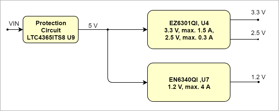
Block Diagram
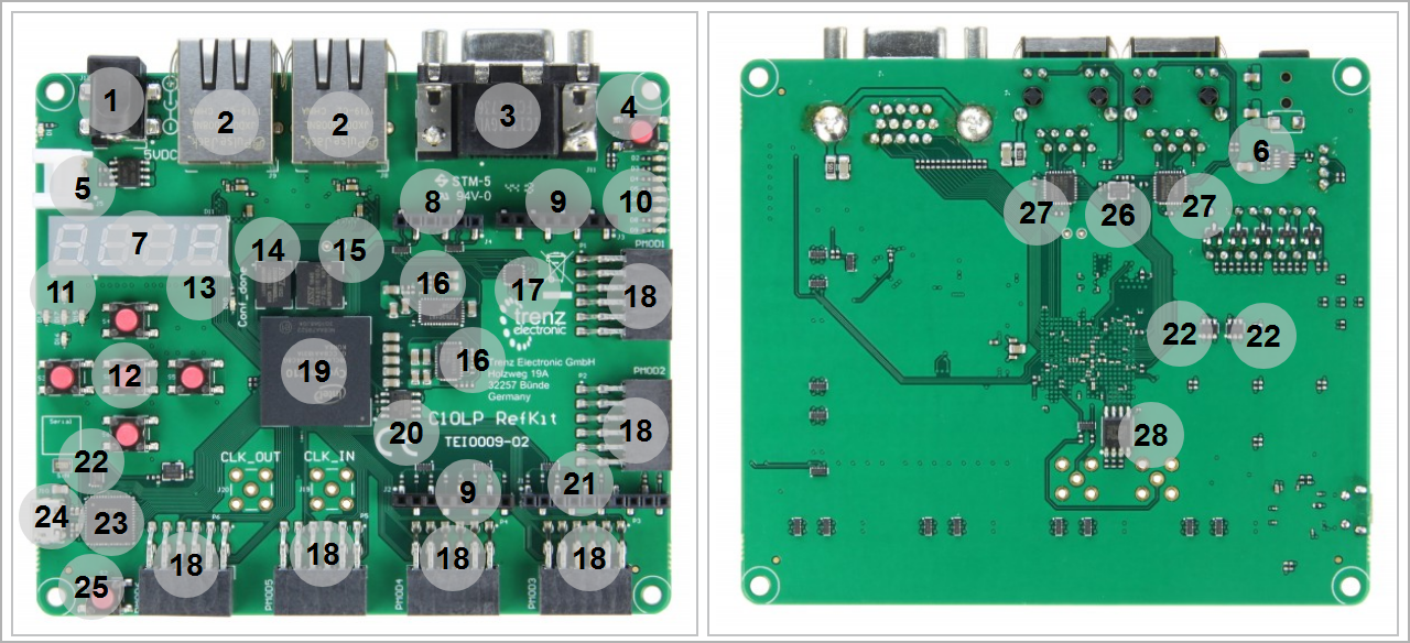
Main Components
Notes : - Picture of the PCB (top and bottom side) with labels of important components
- Add List below
|
- Barrel Jack, J12
- RJ45 socket, J8...9
- VGA Socket, J11
- Push button(Reset), S7
- Grove connector, J5
- Under/Over Voltage Protector, U9
- 7-segment LED, D11
- 1x6 pin header, J4
- 1x8 pin header, J2...3
- User Red LEDs, D2...9
- User Red LEDs, D13...17
- Push buttons, S1- S3...6
- Red LED (CONF_DONE), D10
- PSDRAM memory, U3
- SDRAM memory, U10
- Voltage Regulator, U5- U7
- AD/DA Convertor, U2
- Pmod 2x6 SMD host socket, P1...6
- Intel Cyclone 10 LP, U1
- Config Device, U5
- 1x10 pin header, J1
- EEEPROM, U15- U18- U20
- FTDI FT2232H, U14
- Micro USB 2.0 receotacle 90, J10
- Push button (RST_GPIO), S2
- Oscillator, U22
- Ethernet PHY, U17- U19
- SPI Flash memory, U12
Initial Delivery State
Notes : Only components like EEPROM, QSPI flash and DDR3 can be initialized by default at manufacture. If there is no components which might have initial data ( possible on carrier) you must keep the table empty |

Storage device name | Content | Notes |
|---|
SPI Flash |
|
| | EEPROM |
|
| | DDR3 SDRAM |
|
| | FTDI System Controller CPLD |
|
| | PSDRAM |
|
| | Config Device |
|
|
|
Configuration Signals
- Overview of Boot Mode, Reset, Enables.
|
Configuration mode has been set to AS (Active Serial) configuration.

MODE Signal State | MSEL0 | MSEL1 | MSEL2 | MSEL3 | Connected to | Boot Mode |
|---|
MSEL[0:3] | 0 | 1 | 0 | 0 | Bank 6 | AS (Active Serial) |
|
RESET pin can be set through the push button S1.

Signal | Connected to | Note |
|---|
RESET | S1 (Push button) | Connected to nCONFIG | | EXT_RST | J3 (1x8 pin header) Bank 2 |
|
|
Signals, Interfaces and Pins
Notes : - For carrier or stand-alone boards use subsection for every connector type (add designator on description, not on the subsection title), for example:
- For modules which needs carrier use only classes and refer to B2B connector if more than one is used, for example
|
I/Os on Pin Headers and Connectors
FPGA bank number and number of I/O signals connected to the B2B connector:

| FPGA Bank | Connector | I/O Signal Count | Voltage Level | Notes |
|---|
| Bank 1 | J1 (Pin header) | 8 Single ended | 3.3 V |
| | J2 (Pin header) | 8 Single ended | 3.3 V |
| | J4 (Pin header) | 6 Single ended | 3.3 V |
| | Bank 2 | J3 (Pin header) | 1 Single ended | 3.3 V |
| | P1 (PMod SMD host socket) | 8 Single ended | 3.3 V |
| | P2 (PMod SMD host socket) | 8 Single ended | 3.3 V |
| | J11 (VGA host Socket) | 14 Single ended | 3.3 V |
| | Bank 6 | J5 (Grove connector) | 2 Single ended | 3.3 V |
| | Bank 7 | P5 (PMod SMD host socket) | 8 Single ended | 3.3 V |
| | P6 (PMod SMD host socket) | 8 Single ended | 3.3 V |
| | Bank 8 | P3 (PMod SMD host socket) | 8 Single ended | 3.3 V |
| | P4 (PMod SMD host socket) | 8 Single ended | 3.3 V |
|
|
PMod SMD Host Socket
TEI0009 has 6 PMod 2x6 SMD Host Socket 90° which are connected to Cyclon 10 LP.

| Designator | Signals | Connected to | Notes |
|---|
| P1 | P1_IO1...8 | Bank 2 |
| | P2 | P2_IO1...8 | Bank 2 |
| | P3 | P3_IO1...8 | Bank 8 |
| | P4 | P4_IO1...8 | Bank 8 |
| | P5 | P5_IO1...8 | Bank 7 |
| | P6 | P6_IO1...8 | Bank 7 |
|
|
UART Interface
UART access to TEI0009 is available on 1x8 pin header J2.

| Schematic | Pin Header | Connected to | Voltage Level | Notes |
|---|
| TXD | J2 | Bank 1 | 3.3 V |
| | RXD | J2 | Bank 1 | 3.3 V |
|
|
Micro USB2.0 Connector
U14(FTDI FT2232) can be accessed through Micro USB2.0 B Receptacle 90 (J10).

| Schematic | Connected to | Voltage Level | Notes |
|---|
| USB_VBUS | GND |
|
| | D- | U14 (FTDI FT2232) | 3.3 V |
| | D+ | U14 (FTDI FT2232) | 3.3 V |
|
|
RJ45 Connectors
TEI0009 is equipped with two RJ45 connectors and two Ethernet PHYs. RJ45 connectors J8 and J9 are connected to Ethernet PHYs U17 and U19 respectively. .

| Pin | Schematic | ETH1 Pin | ETH2 Pin | Notes |
|---|
| TD+ | ETH_TX_P | U17- TXP | U19- TXP |
| | CT | ETH_CTREF_TCT | - | - | Connected to GND | | TD- | ETH_TX_N | U17- TXM | U19- TXM |
| | RD+ | ETH_RX_P | U17- RXP | U19- RXP |
| | CT | ETH_CTREF_RCT | - | - | Connected to GND | | RD- | ETH_RX_N | U17- RXM | U19- RXM |
| | LED Green | ETH_LED0 | U17- NWAYEN | U19- NWAYEN |
| | LED Yellow | ETH_LED1 | U17- SPEED | U19- SPEED |
|
|
VGA socket Connectors
VGA host socket is connected to Cyclone 10 LP through Bank 2.

| Schematic | Corresponding Signals | Connected to | Notes |
|---|
| VGA_RED | VGA_R0...3 | Bank 2 | Red channel | | VGA_GREEN | VGA_G0...3 | Bank 2 | Green channel | | VGA_BLUE | VGA_B0...3 | Bank 2 | Blue channel | | VGA_RGB_HSYNC | VGA_HS | Bank 2 | Horizontal sync | | VGA_RGB_VSYNC | VGA_VS | Bank 2 | Vertical sync |
|
On-board Peripherals
Notes : - add subsection for every component which is important for design, for example:
- Two 100 Mbit Ethernet Transciever PHY
- USB PHY
- Programmable Clock Generator
- Oscillators
- eMMCs
- RTC
- FTDI
- ...
- DIP-Switches
- Buttons
- LEDs
|
Notes : In the on-board peripheral table "chip/Interface" must be linked to the corresponding chapter or subsection |

| Chip/Interface | Designator | Notes |
|---|
| SPI Flash memory | U12 |
| | SDRAM memory | U10 |
| | PSDRAM memory | U3 |
| | 7 Segment | D11 |
| | FTDI FT2232 | U14 |
| | Ethernet PHY | U17, U19 |
| | Configuration Device | U5 |
| | AD/DA Converter | U2 |
| | EEPROM | U15, U18, U20 |
| | User LEDs | D2...D17 |
| | Oscillators | U16, U22 |
|
|
Quad SPI Flash Memory
Notes : Minimum and Maximum density of quad SPI flash must be mentioned for other assembly options. |

| MIO Pin | Schematic | U?? Pin | Notes |
|---|
|
|
|
|
|
|
|
|
|
|
|
|
|
|
|
|
|
|
|
|
|
|
|
|
|
RTC

| MIO Pin | Schematic | U? Pin | Notes |
|---|
|
|
|
|
|
|
|
|
|

| MIO Pin | I2C Address | Designator | Notes |
|---|
|
|
|
|
|
EEPROM

| MIO Pin | Schematic | U?? Pin | Notes |
|---|
|
|
|
|
|
|
|
|
|

| MIO Pin | I2C Address | Designator | Notes |
|---|
|
|
|
|
|
LEDs

| Schematic | Color | Connected to | Active Level | Note |
|---|
|
|
|
|
|
|
|
|
|
|
|
|
|
|
|
|
DDR3 SDRAM
Notes : Minimum and Maximum density of DDR3 SDRAM must be mentioned for other assembly options. (pay attention to supported address length for DDR3) |
The TE???? SoM has ??? GByte volatile DDR3 SDRAM IC for storing user application code and data.
- Part number:
- Supply voltage:
- Speed:
- NOR Flash
- Temperature:
Ethernet

| Bank | Signal Name | ETH1 | ETH2 | Signal Description |
|---|
|
|
|
|
|
|
|
|
|
|
|
|
|
|
|
|
|
|
|
|
|
|
|
|
|
|
|
|
|
|
|
|
|
|
|
|
|
|
|
|
|
|
|
|
|
|
|
|
|
|
|
|
|
|
|
|
|
|
|
|
|
|
|
|
|
|
|
|
|
|
|
CAN Transceiver

| Bank | Schematic | U?? Pin | Notes |
|---|
| D-Tx |
| Driver Input |
| R-Rx |
| Reciever Output |
|
Clock Sources

| Designator | Description | Frequency | Note |
|---|
|
| MHz |
|
|
| MHz |
|
|
| KHz |
|
|
|
|
|
|
Power and Power-On Sequence
In 'Power and Power-on Sequence' section there are three important digrams which must be drawn: - Power on-sequence
- Power distribution
- Voltage monitoring circuit
|
Power Supply
Power supply with minimum current capability of xx A for system startup is recommended.
Power Consumption

| Power Input Pin | Typical Current |
|---|
| VIN | TBD* |
|
* TBD - To Be Determined
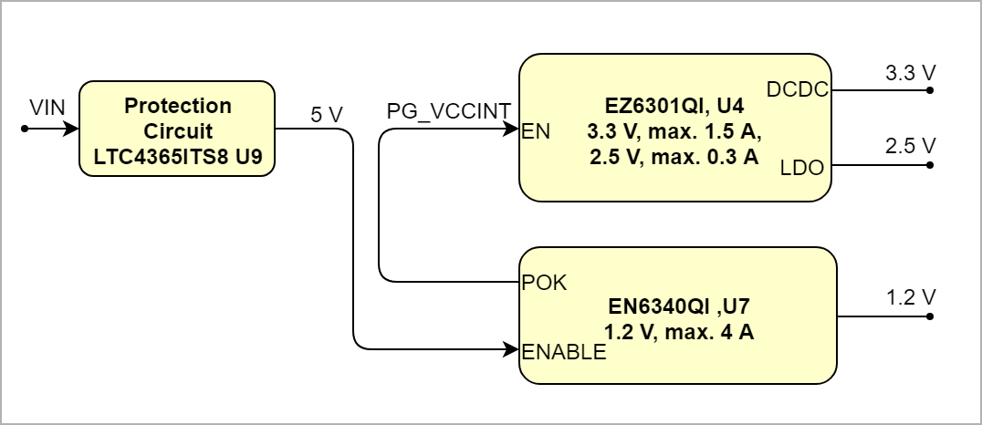
Power Distribution Dependencies
Power-On Sequence
Voltage Monitor Circuit
Create DrawIO object here: Attention if you copy from other page, objects are only linked. |
image link to the generate DrawIO PNG file of this page. This is a workaround until scroll pdf export bug is fixed |
|
Power Rails

| Power Rail Name | B2B Connector JM1 Pin | B2B Connector JM2 Pin | B2B Connector JM3 Pin | Direction | Notes |
|---|
|
|
|
|
|
|
|
|
|
|
|
|
|
|
|
|
|
|
|
|
|
|
|
|
|
Bank Voltages
Board to Board Connectors
- This section is optional and only for modules.
use "include page" macro and link to the general B2B connector page of the module series, For example: 6 x 6 SoM LSHM B2B Connectors

|
? x ? modules use two or three Samtec Micro Tiger Eye Connector on the bottom side.
3 x REF-??????? (compatible to ????????), (?? pins, ?? per row)
Operating Temperature: -??°C ~ ??°C
Current Rating: ??A per ContactNumber of Positions: ??
Number of Rows: ??
Technical Specifications
Absolute Maximum Ratings

| Symbols | Description | Min | Max | Unit |
|---|
|
|
|
| V |
|
|
|
| V |
|
|
|
| V |
|
|
|
| V |
|
|
|
| V |
|
|
|
| V |
|
|
|
| V |
|
|
|
| V |
|
|
|
|
|
|
|
|
|
|
|
Recommended Operating Conditions
Operating temperature range depends also on customer design and cooling solution. Please contact us for options.

| Parameter | Min | Max | Units | Reference Document |
|---|
|
|
| V | See ???? datasheets. |
|
|
| V | See Xilinx ???? datasheet. |
|
|
| V | See Xilinx ???? datasheet. |
|
|
| V | See Xilinx ???? datasheet. |
|
|
| V | See Xilinx ???? datasheet. |
|
|
| V | See Xilinx ???? datasheet. |
|
|
| V | See Xilinx ???? datasheet. |
|
|
| °C | See Xilinx ???? datasheet. |
|
|
| °C | See Xilinx ???? datasheet. |
|
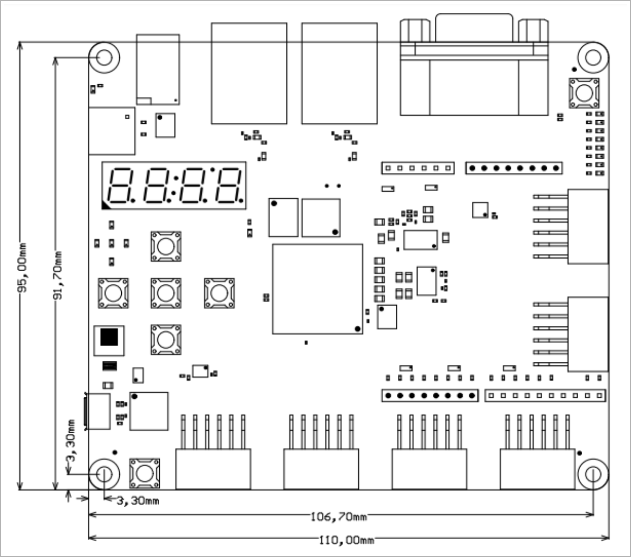
Physical Dimensions
PCB thickness: ?? mm.
Currently Offered Variants
Revision History
Hardware Revision History

| Date | Revision | Changes | Documentation Link |
|---|
| - |
|
|
|
|
|
|
|
|
Hardware revision number can be found on the PCB board together with the module model number separated by the dash.
Create DrawIO object here: Attention if you copy from other page, objects are only linked. |
image link to the generate DrawIO PNG file of this page. This is a workaround until scroll pdf export bug is fixed |
|
Document Change History
- Note this list must be only updated, if the document is online on public doc!
- It's semi automatically, so do following
Add new row below first Copy "Page Information Macro(date)" Macro-Preview, Metadata Version number, Author Name and description to the empty row. Important Revision number must be the same as the Wiki document revision number Update Metadata = "Page Information Macro (current-version)" Preview+1 and add Author and change description. --> this point is will be deleted on newer pdf export template - Metadata is only used of compatibility of older exports
|

| Date | Revision | Contributor | Description |
|---|
| | 
| | -- | all | 
| |
|
Disclaimer


