Template Revision 2.12
- Module: TRM Name always "TE Series Name" +TRM
Example: "TE0728 TRM" - Carrier: TRM Name usually "TEB Series Name" +TRM
Example: "TEB0728 TRM"
|
<!-- tables have all same width (web max 1200px and pdf full page(640px), flexible width or fix width on menu for single column can be used as before) -->
<style>
.wrapped{
  width: 100% !important;
  max-width: 1200px !important;
 }
</style> |
----------------------------------------------------------------------- |
Note for Download Link of the Scroll ignore macro: |
Table of Contents 
|
Overview
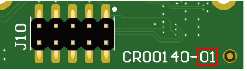
The Trenz Electronic CR00140-01 is a CRUVI motor driver module. It supports motors with up to 4 phases up to 40V.
Refer to http://trenz.org/ for the current online version of this manual and other available documentation.
Key Features
Note:
'description: Important components and connector or other Features of the module
→ please sort and indicate assembly options Key Features' must be split into 6 main groups for modues: - SoC/FPGA
- Package:
- Speed:
- Temperature:
- RAM/Storage
- On Board
- Interface
- E.g. ETH, USB, B2B, Display port
- Power
- E.g. Input supply voltage
- Dimension
Key Features' must be split into 6 main groups for carrier: - Modules
- TE0808, TE807, TE0803,...
- RAM/Storage
- On Board
- Interface
- E.g. ETH, USB, B2B, Display port
- Power
- E.g. Input supply voltage
- Dimension
|
- On Board
- MAX10 CPLD
- 2 phase current measurement
- DC_LINK voltage measurement
- 4x LEDs (2 power indicator, 2 user)
- 2x Pushbutton
- EEPROM
- Interface
- 4 phase screw terminal motor connector
- CRUVI for control
- 6x1 pin header for single ended sensors
- 5x2 pin header for differential sensors
- Power
- screw terminal for up to 40 V DC motor supply
- Dimension
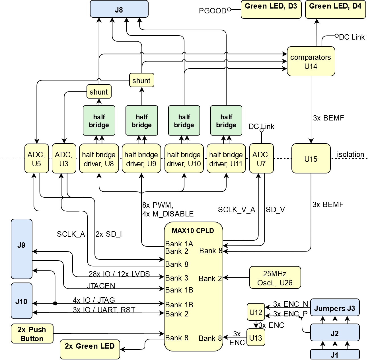
Block Diagram
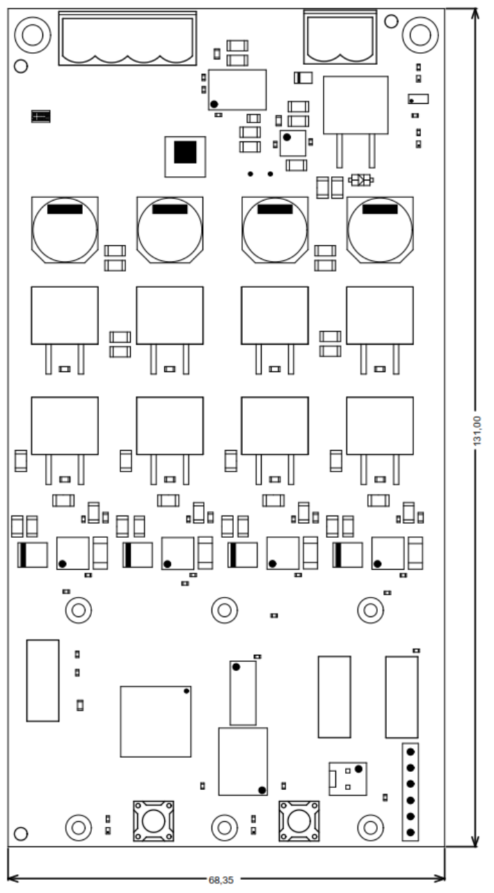
Main Components
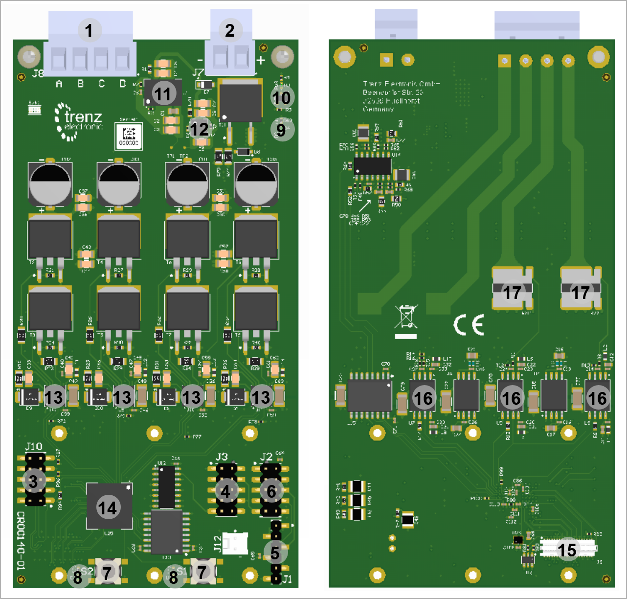
Notes : - Picture of the PCB (top and bottom side) with labels of important components
- Add List below
|
- Motor connector screw terminal, J8
- Power supply screw terminal, J7
- 5x2 pinheader, base for TEI0004 JTAG programmer, J10
- 5x2 pinheader for sensor selection, J3
- 6x1 pinheader for single ended sensors, J1
- 5x2 pinheader for differential sensors, J2
- User push buttons, S1, S2
- User LEDs, D1, D2
- LED DC_Link, D4
- LED Power Good, D3
- DCDC for 15V, U1
- DCDC for 5V, U2
- half bridge drivers, U8, U9, U10, U11
- MAX10 CPLD, U25
- CRUVI high speed connector
- ADCs, U3, U5, U7
- Shunt resistors, R22, R28
Initial Delivery State
Notes : Only components like EEPROM, QSPI flash can be initialized by default at manufacture. If there is no components which might have initial data ( possible on carrier) you must keep the table empty |

Storage device name | Content | Notes |
|---|
| MAX10 CPLD | default firmware REV01 | See firmware documentation |
|
Signals, Interfaces and Pins
Notes : - For carrier or stand-alone boards use subsection for every connector type (add designator on description, not on the subsection title), for example:
- For modules which needs carrier use only classes and refer to B2B connector if more than one is used, for example
|
Board to Board (B2B) I/Os
FPGA bank number and number of I/O signals connected to the B2B connector:
| CPLD Bank | B2B Connector | I/O Signal Count | Voltage Level | Notes |
|---|
| 3 | J9 | 12 x LVDS / 24 I/Os | VADJ | 6 x RX + 6 x TX | | 3 | J9 | 4 I/Os | VADJ |
| | 8 | J9 | 4 I/Os | 3.3V | Constant 3.3V | | 1B | J9 | 5 I/Os | 3.3V | JTAG, JTAGEN, Constant 3.3V |
|
JTAG Interface
JTAG access to the CPLD of CR00140 is possible via the CRUVI high speed connector J9 and the pinheader J10, which is a base for TEI004 JTAG programmer. The JTAGEN signal is pulled up and available on J9 only. If JTAGEN is pulled low, the four signals can be used as user I/Os.
JTAG Signal | B2B Connector | Pin header | Notes |
|---|
| TMS | J9-55 | J10-5 | pull up | | TDI | J9-51 | J10-9 | pull up | | TDO | J9-53 | J10-3 | - | | TCK | J9-59 | J10-1 | pull down | | JTAGEN | J9-57 | - | high for enable JTAG port of CPLD, low for user I/Os, pull up | | UART_RX | - | J10-7 | CPLD Firmware dependent, see Firmware | | UART_TX | - | J10-8 | CPLD Firmware dependent, see Firmware | | RST | - | J10-6 | CPLD Firmware dependent, see Firmware | | +3.3V_D | J9-4, J9-9 | J10-4 | - | | DGND | several, see CRUVI | J10-2, J10-10 | - |
|
Sensor Interface
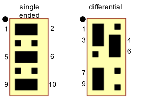
The pin headers J1, J2 and J3 constitute the sensor interface. It can be e.g. used with Encoders or Hall sensors. J3 is the selector between differential sensor interface (J2) or single ended sensors (J1). Connecting sensors is only allowed to one of the two pinheaders (J1/J2), the other one has to stay unconnected. In the figure below the jumper configuration of J3 to enable one or the other type of sensor interface is depicted.
The pinheaders for connection of the sensors are further described in the following table. For differential configuration 100 Ohm parallel termination is used.
Signal | J1 pin (singel ended) | J2 pin (differential) |
|---|
| ISO_ENC_A_P | 3 | 6 | | ISO_ENC_A_N | - | 5 | | ISO_ENC_B_P | 5 | 8 | | ISO_ENC_B_N | - | 7 | | ISO_ENC_I_P | 2 | 10 | | ISO_ENC_I_N | - | 9 | | DGND | 4 | 3 | | +5.0V_D | 1, 6 | 2 |
|
Motor Interface
CR00140 has a motor interface, where up to 4 phases can be driven.
Check carefully correct connection of the phases of the motor, according to the motor and the implemented driving algorithm. |
Signal | J8 pin lable | Note |
|---|
| Motor_A | A | Current measurement via R22 and ADC U3 | | Motor_B | B | Current measurement via R28 and ADC U5 | | Motor_C | C | - | | Motor_D | D | - |
|
CRUVI
For the connection to a control unit, the CRUVI interface is implemented. One high speed connector J9 is assembled. The connectors are further described in section B2B Connectors. The connection of the signals and the voltage levels is described in the CPLD section.
Signal | Connector - Pin |
|---|
| DGND | J9-12, J9-18, J9-24, J9-30, J9-42, J9-48, J9-54, J9-13, J9-19, J9-25, J9-31, J9-37, J9-43, J9-49 | +3.3V_D | J9-4, J9-9 | | +5.0V_D | J9-60 | | VADJ | J9-36 | | A0_P | J9-14 | | A0_N | J9-16 | | A1_P | J9-20 | | A1_N | J9-22 | | A2_P | J9-26 | | A2_N | J9-28 | | A3_P | J9-32 | | A3_N | J9-34 | | A4_P | J9-38 | | A4_N | J9-40 | | A5_P | J9-44 | | A5_N | J9-46 | | B0_P | J9-15 | | B0_N | J9-17 | | B1_P | J9-21 | | B1_N | J9-23 | | B2_P | J9-27 | | B2_N | J9-29 | | B3_P | J9-33 | | B3_N | J9-35 | | B4_P | J9-39 | | B4_N | J9-41 | | B5_P | J9-45 | | B5_N | J9-47 | | HSIO | J9-2 | | HSO | J9-6 | | RESET | J9-8 | | HSI | J9-10 | TDI | J9-51 | | TDO | J9-53 | | TMS | J9-55 | | JTAGEN | J9-57 | | TCK | J9-59 | | SMB_ALERT | J9-3 | | SMB_SDA | J9-5 | | SMB_SCL | J9-7 | | REFCLK | J9-11 |
|
On-board Peripherals
Notes : - add subsection for every component which is important for design, for example:
- Two 100 Mbit Ethernet Transciever PHY
- USB PHY
- Programmable Clock Generator
- Oscillators
- eMMCs
- RTC
- FTDI
- ...
- DIP-Switches
- Buttons
- LEDs
|
CPLD
A Intel/Altera MAX10 FPGA 10M08SAU169C8G (U25) is used as system controller. Table below lists the SC CPLD I/O signals and pins.
| Signal name | SC CPLD Pin | CPLD Bank | Connected to | Function | Notes |
|---|
| A0_P | J8 | 3 | J9-14 | CPLD firmware dependent | See CPLD Firmware | | A0_N | K8 | 3 | J9-16 | CPLD firmware dependent | See CPLD Firmware | | A1_P | M13 | 3 | J9-20 | CPLD firmware dependent | See CPLD Firmware | | A1_N | M12 | 3 | J9-22 | CPLD firmware dependent | See CPLD Firmware | | A2_P | M9 | 3 | J9-26 | CPLD firmware dependent | See CPLD Firmware | | A2_N | M8 | 3 | J9-28 | CPLD firmware dependent | See CPLD Firmware | | A3_P | N8 | 3 | J9-32 | CPLD firmware dependent | See CPLD Firmware | | A3_N | N7 | 3 | J9-34 | CPLD firmware dependent | See CPLD Firmware | | A4_P | M7 | 3 | J9-38 | CPLD firmware dependent | See CPLD Firmware | | A4_N | N6 | 3 | J9-40 | CPLD firmware dependent | See CPLD Firmware | | A5_P | K5 | 3 | J9-44 | CPLD firmware dependent | See CPLD Firmware | | A5_N | J5 | 3 | J9-46 | CPLD firmware dependent | See CPLD Firmware | | B0_P | N5 | 3 | J9-15 | CPLD firmware dependent | See CPLD Firmware | | B0_N | N4 | 3 | J9-17 | CPLD firmware dependent | See CPLD Firmware | | B1_P | J7 | 3 | J9-21 | CPLD firmware dependent | See CPLD Firmware | | B1_N | K7 | 3 | J9-23 | CPLD firmware dependent | See CPLD Firmware | | B2_P | L11 | 3 | J9-27 | CPLD firmware dependent | See CPLD Firmware | | B2_N | M11 | 3 | J9-29 | CPLD firmware dependent | See CPLD Firmware | | B3_P | L10 | 3 | J9-33 | CPLD firmware dependent | See CPLD Firmware | | B3_N | M10 | 3 | J9-35 | CPLD firmware dependent | See CPLD Firmware | | B4_P | J6 | 3 | J9-398 | CPLD firmware dependent | See CPLD Firmware | | B4_N | K6 | 3 | J9-41 | CPLD firmware dependent | See CPLD Firmware | | B5_P | L5 | 3 | J9-45 | CPLD firmware dependent | See CPLD Firmware | | B5_N | L4 | 3 | J9-47 | CPLD firmware dependent | See CPLD Firmware | | HSIO | N9 | 3 | J9-2 | CPLD firmware dependent | See CPLD Firmware | | HSO | N10 | 3 | J9-6 | CPLD firmware dependent | See CPLD Firmware | | RESET | M5 | 3 | J9-8 | CPLD firmware dependent | See CPLD Firmware | | HSI | N12 | 3 | J9-10 | CPLD firmware dependent | See CPLD Firmware | TDI | F5 | 1B | J9-51, J10-9 | JTAG / user IO CPLD firmware dependent | See CPLD Firmware | | TDO | F6 | 1B | J9-53, J10-3 | JTAG / user IO CPLD firmware dependent | See CPLD Firmware | | TMS | G1 | 1B | J9-55, J10-5 | JTAG / user IO CPLD firmware dependent | See CPLD Firmware | | JTAGEN | E5 | 1B | J9-57 | JTAG enable CPLD firmware dependent | See CPLD Firmware | | TCK | G2 | 1B | J9-59, J10-1 | JTAG / user IO CPLD firmware dependent | See CPLD Firmware | | SMB_ALERT | K2 | 2 | J9-3 | CPLD firmware dependent | See CPLD Firmware | | SMB_SDA | H5 | 2 | J9-5 | CPLD firmware dependent | See CPLD Firmware | | SMB_SCL | H4 | 2 | J9-7 | CPLD firmware dependent | See CPLD Firmware | | REFCLK | M2 | 2 | J9-11 | CPLD firmware dependent | See CPLD Firmware | | BUTTON1 | C10 | 8 | S2 | CPLD firmware dependent | activ low, See CPLD Firmware | | BUTTON2 | B10 | 8 | S1 | CPLD firmware dependent | activ low, See CPLD Firmware | | ENC_A | A10 | 8 | U13-13 | Sensor input channel A | - | | ENC_B | A9 | 8 | U13-12 | Sensor input channel B | - | | ENC_I | A11 | 8 | U13-14 | Sensor input channel I | - | | LED0 | D6 | 8 | D2 | CPLD firmware dependent | See CPLD Firmware | | LED1 | B2 | 8 | D1 | CPLD firmware dependent | See CPLD Firmware | | M_BEMF_B_D | B5 | 8 | U15-13 | Back EMF signal phase B | - | | M_BEMF_C_D | A5 | 8 | U15-12 | Back EMF signal phase C | - | | M_BEMF_A_D | A4 | 8 | U15-14 | Back EMF signal phase A | - | | M_PWM_AH | F1 | 1A | U8-2 | Phase A half bridge high (DC_LINK) side driver signal | - | | M_PWM_AL | E3 | 1A | U8-3 | Phase A half bridge low (PGND) side driver signal | - | | M_PWM_BH | E1 | 1A | U9-2 | Phase B half bridge high (DC_LINK)side driver signal | - | | M_PWM_BL | D1 | 1A | U9-3 | Phase B half bridge low (PGND) side driver signal | - | | M_PWM_CH | E4 | 1A | U10-2 | Phase C half bridge high (DC_LINK)side driver signal | - | | M_PWM_CL | C1 | 1A | U10-3 | Phase C half bridge low (PGND) side driver signal | - | | M_PWM_DH | C2 | 1A | U11-2 | Phase D half bridge high (DC_LINK) side driver signal | - | | M_PWM_DL | B1 | 1A | U11-3 | Phase D half bridge low (PGND) side driver signal | - | | SD_IA | E6 | 8 | U3-6 | Current measurement phase A | 33 Ohm series Resistor | | SCLK_A | B3 | 8 | U3-7, U5-7 | Clock for ADC for current measurement phase A and B | (5-20 MHz) | | SD_V | B4 | 8 | U7-6 | Voltage measurement DC_LINK | 33 Ohm series Resistor | | SD_IB | A2 | 8 | U5-6 | Current measurement phase B | 33 Ohm series Resistor | | SCLK_V_A | A3 | 8 | U7-7 | Clock for ADC for voltage measurement DC_LINK | (5-20 MHz) | | M_DISABLE_D_D | J1 | 2 | U11-5 | Halfe bridge disable phase D | disabled when high, pull up connected | | M_DISABLE_A_D | M1 | 2 | U8-5 | Halfe bridge disable phase A | disabled when high, pull up connected | | M_DISABLE_B_D | L2 | 2 | U9-5 | Halfe bridge disable phase B | disabled when high, pull up connected | | M_DISABLE_C_D | K1 | 2 | U10-5 | Halfe bridge disable phase C | disabled when high, pull up connected | | REFCLK | M2 | 2 | J9-11 | CPLD firmware dependent | - | | RST | M3 | 2 | J10-6 | CPLD firmware dependent | - | | UART_RX | N2 | 2 | J10-7 | CPLD firmware dependent | - | | UART_TX | N3 | 2 | J10-8 | CPLD firmware dependent | - | | CLK_25MHZ | H6 | 2 | U26-3 | Clock input for accurate 25 Mhz clk. | - |
|
CPLD Bank Voltages
| Schematic Name | | Notes |
|---|
| 1A | +3.3V_D | 3.3V | Provided via CRUVI | | 1B | +3.3V_D | 3.3V | Provided via CRUVI | | 2 | +3.3V_D | 3.3V | Provided via CRUVI | | 3 | VADJ | 1.8V, 2.5V, 3.3V | Provided via CRUVI, supported voltage levels are determined by the CPLD Firmware, and the connected base/controller. | | 8 | +3.3V_D | 3.3V | Provided via CRUVI |
|
LEDs
| Designator | Color | Connected to | Signal name | Active Level | Note |
|---|
| D1 | green | U25-B2 | LED1 | high | User LED, CPLD Firmware dependent, see Firmware description. | | D2 | green | U25-D6 | LED0 | high | User LED, CPLD Firmware dependent, see Firmware description. | | D3 | green | U1-A3, U2-B1 | PGOOD | high | ON when +15.0V_M and +5.0V_M regulator indicated power good. Connected via transistor T1. | | D4 | green | DC_LINK | - | low | ON when DC_LINK above 11.7V. Connected via comparator U14D to DC_LINK |
|
Buttons
| Designator | Connected to | Signal name | Active Level | Note |
|---|
| S1 | U25-B10 | BUTTON2 | low | User button, CPLD Firmware dependent, see Firmware description. | | S2 | U25-C10 | BUTTON1 | low | User button, CPLD Firmware dependent, see Firmware description. |
|
ADCs
There are three isolating AD7403-8 ADCs for continous measurement oft phase A current (U3), phase B current (U5) and the DC_LINK voltage (U7) on board. The currents are measured through the shunt resistors R22, R28 for phase A and B respectively. The ADC clock is routed to the CPLD. For Currents the clock has the signal lable SCLK_A and for the voltage SCLK_V_A. The data signals are also routed to the CPLD. See CPLD Firmware for further description.
BEMF
Back EMF zero crossing signals for sensor-less motor control are implemented for Phase A, B and C. They are routed via a triple channel Digital isolator (U15) to the CPLD. See CPLD Firmware for further description.
Half bridge drivers
Four ADuM7223 isolated half bridge drivers (U8, U9, U10, U11) are used for driving the four phases.
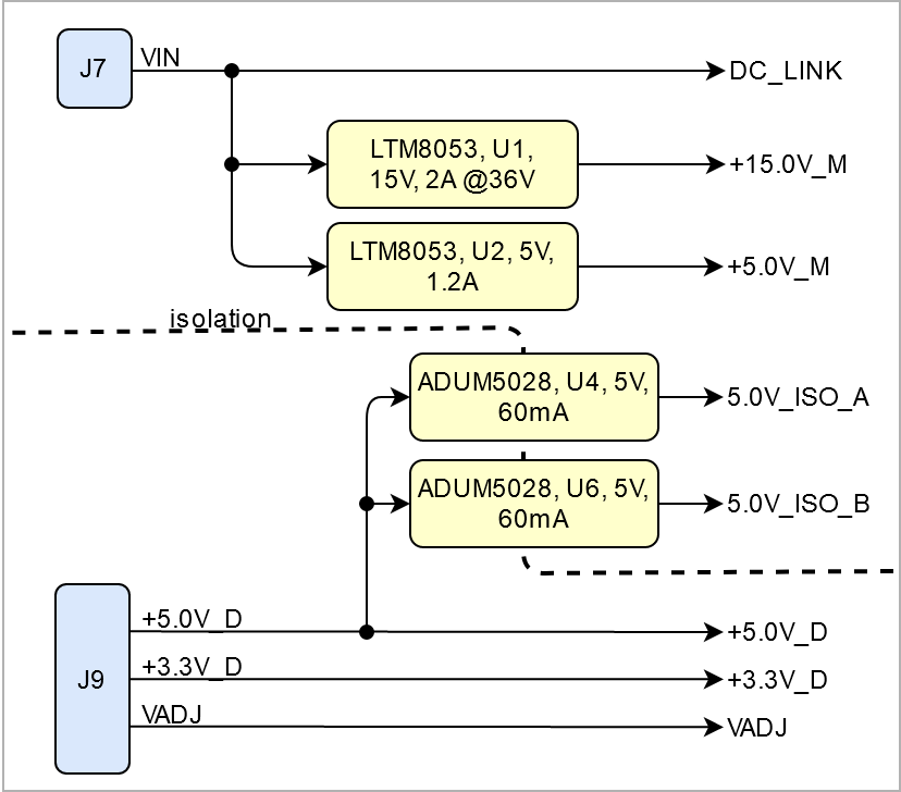
DCDCs
On the Motor side are two DCDCs on board. LTM8053 (U1) is utilized for the generation of the 15V transistor control voltage from VIN and can be measured on Testpoint TP1. A LTM8074 DCDC (U2) generates 5V from VIN for miscellaneous signals on the motor side of the PCB and can be measured on TP2.
Two isolated DCDCs ADUM5028 (U4, U6) are used for the generation two seperate clean 5V for the supply of the current measurement ADCs U3 and U5.
Power and Power-On Sequence
In 'Power and Power-on Sequence' section there are three important digrams which must be drawn: - Power on-sequence
- Power distribution
- Voltage monitoring circuit
|
EEPROM
The 2K Microchip 24AA02E48 EEPROM with pre-programmed unique 48bit address is connected to the CRUVI HS (Signals: SMB_SDA, SMB_SCL) connector and can e.g. be used for identifiction purposes.
Power Supply
The motor driving stage is supplied via connector J7 with maximum of 40V DC. Polarity of the powersupply is noted on the PCB.
Check powersupply for correct polarity. Inversion of polarity will damage the module. At least Transistor T11 may be harmed. Furthermore make sure that under any circumstances the absolute maximum voltage does not exceed 42V. |
Power Consumption
The power consumption on the motor stage side (J7) is dominated by the connected motor and the corresponding driving algorithm. The idle consumption is given below.
| Power Input Pin | Typical Current | Note |
|---|
| VIN | ~ 47mA | @24V (J7), no motor connected, no PWM signal driven. |
|
Power Distribution Dependencies
Power-On Sequence
There is no power on sequence which has to be maintained.
Power Rails
| Power Rail Name | B2B Connectors
| Direction | Notes |
|---|
+3.3V_D | J9-4, J9-9 | In | - | | +5.0V_D | J9-60 | In | - | | VADJ | J9-36 | In | - | | VIN | J7 | In | isolated |
|
Board to Board Connectors
- This section is optional and only for modules.
use "include page" macro and link to the general B2B connector page of the module series, For example: 6 x 6 SoM LSHM B2B Connectors

|

Technical Specifications
Absolute Maximum Ratings
| Symbols | Description | Min | Max | Unit |
|---|
| VIN | Motor supply voltage | 0 | 42 | V | +3.3V_D | digital part 3.3V supply voltage | -0.3 | 3.9 | V | | +5.0V_D | digital part 5V supply voltage | -0.3 | 6.0 | V | | VADJ | IO Bank Voltage | -0.3 | 3.9 | V |
|
Recommended Operating Conditions
Operating temperature range depends also on customer design and cooling solution. Please contact us for options.
| Parameter | Min | Max | Units | Reference Document |
|---|
| VIN | 22 | 40 | V | LTM8053 datasheet | +3.3V_D | 3.135 | 3.465 | V | MAX10 datasheet | | +5.0V_D | 4.75 | 5.25 | V | SN65LBC173AD datasheet | VADJ (3.3V operation) VADJ (2.5V operation) VADJ (1.8V operation) | 3.135 2.375 1.71 | 3.465 2.625 1.89 | V | MAX10 datasheet | | T | -40 | 105 | °C | AD7403-8 (junction) | | T (ambient) | -40 | 85 | °C | SN65LBC173AD datasheet |
|
Physical Dimensions
PCB thickness: 1.6 mm.
Currently Offered Variants
Revision History
Hardware Revision History
| Date | Revision | Changes | Documentation Link |
|---|
| 2019-12-20 | 01 | Prototypes | - | | 2020-03-10 | 02 | removed LS connector J11, added EEPROM U16 | - |
|
Hardware revision number can be found on the PCB board together with the module model number separated by the dash.
Document Change History
- Note this list must be only updated, if the document is online on public doc!
- It's semi automatically, so do following
Add new row below first Copy "Page Information Macro(date)" Macro-Preview, Metadata Version number, Author Name and description to the empty row. Important Revision number must be the same as the Wiki document revision number Update Metadata = "Page Information Macro (current-version)" Preview+1 and add Author and change description. --> this point is will be deleted on newer pdf export template - Metadata is only used of compatibility of older exports
|
| Date | Revision | Contributor | Description |
|---|
| | 
| | -- | all | 
| |
|
Disclaimer